Semiconductor packages and methods of manufacturing the same

a technology of semiconductors and packages, applied in the direction of semiconductor devices, semiconductor/solid-state device details, electrical apparatus, etc., can solve the problems of limited minimum bond pitch, poor mechanical adhesion characteristics of materials suitable for use as solder bumps, and unfavorable work of materials used in each of the techniques

Inactive Publication Date: 2009-07-23
SAMSUNG ELECTRONICS CO LTD
View PDF3 Cites 21 Cited by
  • Summary
  • Abstract
  • Description
  • Claims
  • Application Information

AI Technical Summary

Problems solved by technology

A recent application device of an integrated circuit requires a number of I / O pins, but a number of I / O pins causes many problems with relation to a conventional wire bonding package.
As the number of I / O pins increases, there is a limitation of a minimum bond pitch that occurs by a limited size of a substrate.
However, some characteristics of materials used in each of the techniques are unfavorable to work with.
Materials suitable for use as solder bumps have poor characteristics of mechanical adhesion.
Thus, a material like copper, for example, is a good soldering material but is not well selected for the use of a wire bonding, One reason it that copper easily forms an oxide layer that provides a bad bonding characteristic.
However, corrosive agents for removing the oxide layer are very strong, so that aluminum disposed under an oxide layer is also corroded.
However, gold disposed on a solder bump pad is easily diffused into adjacent copper or adjacent solder and forms not only a void but also forms an undesired intermetallic compound that is vulnerable to an impact.

Method used


Image

  • Semiconductor packages and methods of manufacturing the same
  • Semiconductor packages and methods of manufacturing the same
  • Semiconductor packages and methods of manufacturing the same

Examples


Embodiment Construction

[0037]The present general inventive concept now will be described more fully hereinafter with reference to the accompanying drawings, in which embodiments of the present general inventive concept are illustrated. The present general inventive concept may, however, be embodied in many different forms and should not be construed as limited to the embodiments set forth herein. Rather, these embodiments are provided so that this disclosure will be thorough and complete, and will fully convey the scope of the present general inventive concept to those skilled in the art. In the drawings, the size and relative sizes of layers and regions may be exaggerated for clarity. Like numbers refer to like elements throughout.

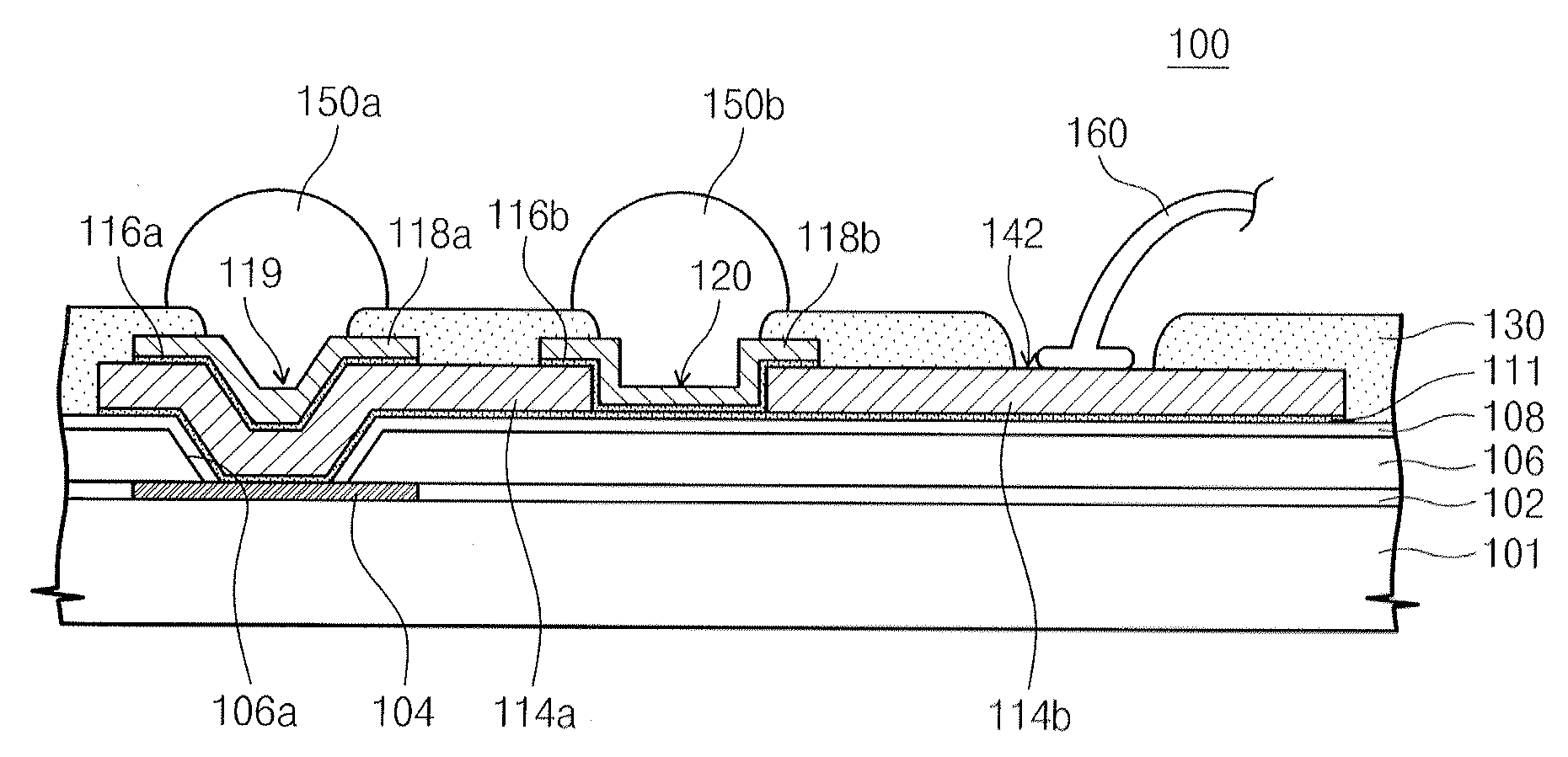
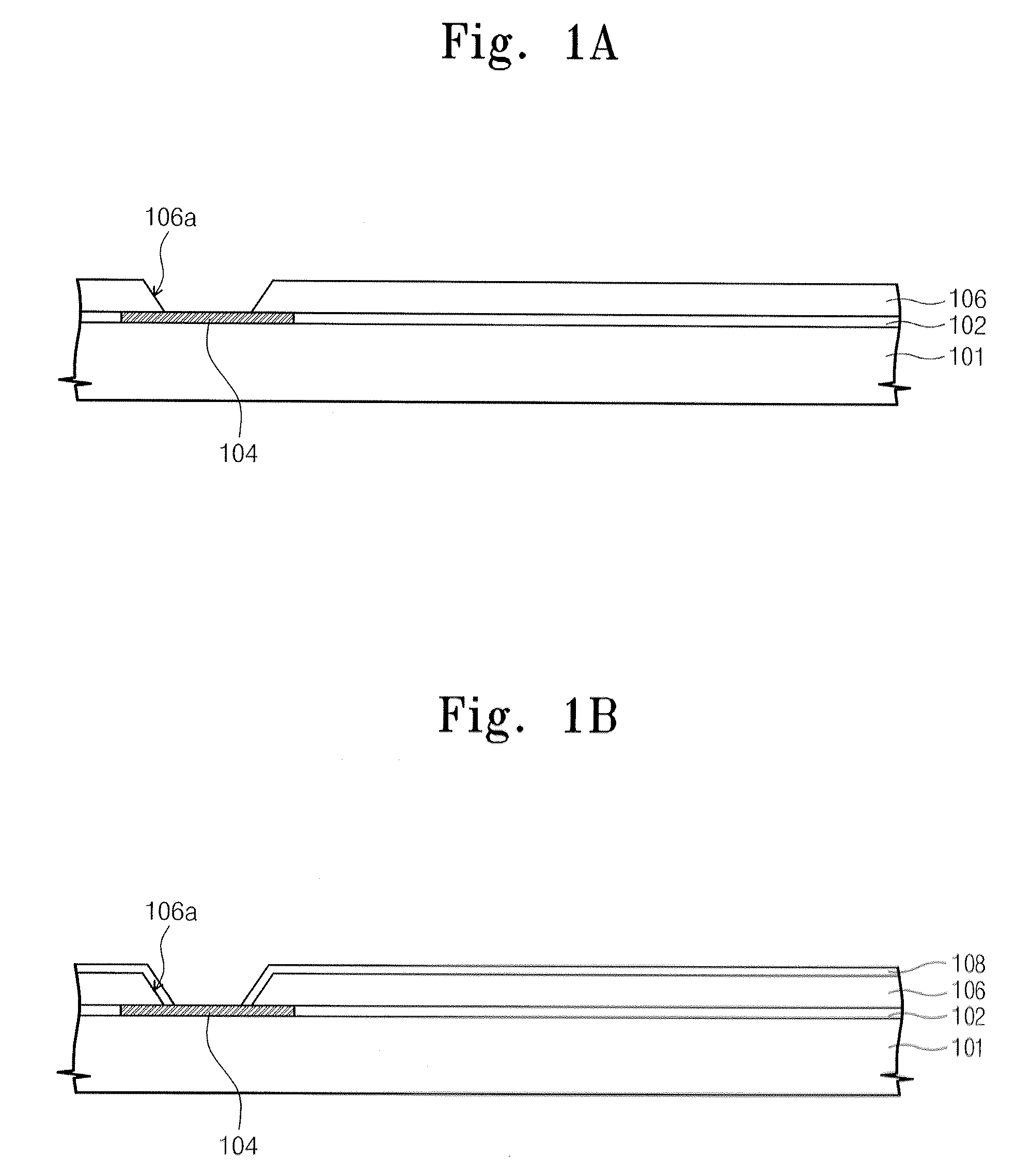
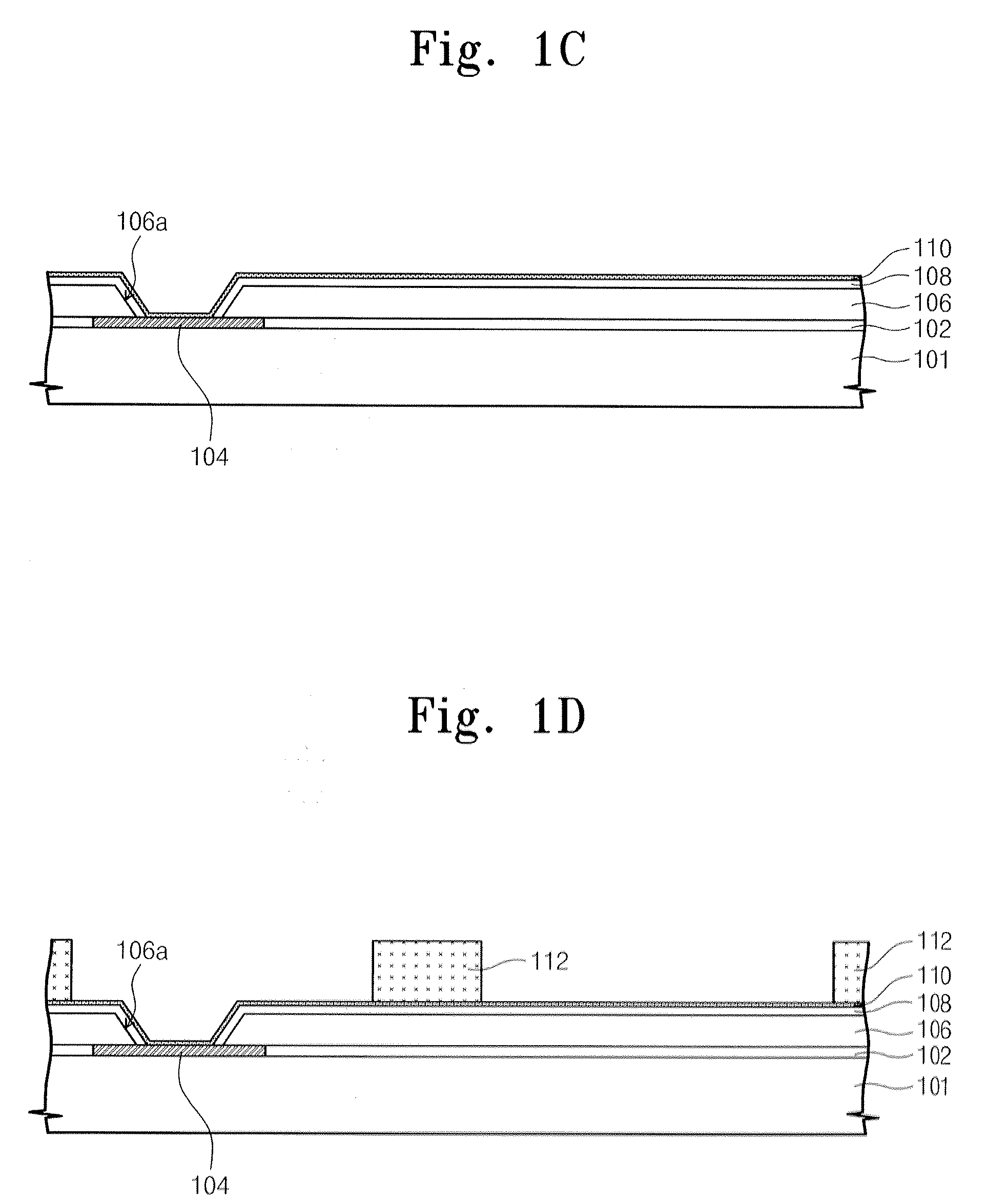
[0038]FIGS. 1A through 1K are cross-sectional views illustrating a method of manufacturing a semiconductor package according to an embodiment of the present general inventive concept.

[0039]Referring to FIG. 1A, a substrate 101 including an integrated circuit (not illustrated) i...


PUM


Abstract

Provided are semiconductor packages and methods of manufacturing the semiconductor package. The semiconductor packages may include a substrate including a chip pad, a redistributed line which is electrically connected to the chip pad and includes an opening. The semiconductor packages may also include an external terminal connection portion, and an external terminal connection pad which is disposed at an opening and electrically connected to the redistributed line. The present general inventive concept can solve the problem where an ingredient of gold included in a redistributed line may be prevented from being diffused into an adjacent bump pad to form a void or an undesired intermetallic compound. In a chip on chip structure, a plurality of bumps of a lower chip are connected to an upper chip to improve reliability, diversity and functionality of the chip on chip structure.

Description

CROSS-REFERENCE TO RELATED APPLICATIONS[0001]This U.S. non-provisional patent application claims priority under 35 U.S.C. §119 of Korean Patent Application No. 2008-0006703, filed on Jan. 22, 2008, the entire contents of which are hereby incorporated by reference.BACKGROUND OF THE INVENTION[0002]1. Field of the Invention[0003]Exemplary embodiments disclosed herein relate to semiconductor packages and methods of manufacturing the same, and more particularly, to semiconductor packages including two kinds of pads to which different kinds of external terminals are connected, and methods of manufacturing the same.[0004]2. Description of the Related Art[0005]A trend in the recent electronics industry is to manufacture a semiconductor device economically which is small, light, speedy, highly reliable, and highly efficient. One of the techniques which can manufacture the recently innovated semiconductor devices are semiconductor packaging techniques.[0006]A recent application device of an i...

Claims


Application Information

Patent Timeline
Patent Type & Authority Applications(United States)
IPC IPC(8): H01L23/48
CPCH01L24/03H01L2224/02166H01L24/11H01L24/73H01L24/91H01L25/0657H01L2224/0401H01L2224/04042H01L2224/05599H01L2224/13099H01L2224/16145H01L2224/45144H01L2224/48091H01L2224/48227H01L2224/48463H01L2924/01005H01L2924/01013H01L2924/01014H01L2924/01022H01L2924/01028H01L2924/01029H01L2924/01075H01L2924/01078H01L2924/01079H01L2924/01327H01L2924/014H01L2924/14H01L2924/15311H01L24/05H01L2924/10253H01L2225/06568H01L2225/06513H01L2225/0651H01L2924/00014H01L2924/01033H01L2924/01024H01L2924/01006H01L2924/00H01L2224/023H01L2924/0001H01L23/48
Inventor CHUNG, HYUN-SOOCHO, JAE-SHINLEE, DONG-HOJANG, DONG-HYEONHWANG, SEONG-DEOKBAEK, SEUNG-DUK
Owner SAMSUNG ELECTRONICS CO LTD
Why Eureka
Try Eureka