Semiconductor memory device and method of manufacturing semiconductor device with chip on chip structure

a memory device and semiconductor technology, applied in the field of semiconductor memory devices, can solve the problems of single package structure, transfer rate and power consumption, increase in process cost, etc., and achieve the effect of improving design and production efficiency

Inactive Publication Date: 2005-04-12
CETUS TECH INC
View PDF5 Cites 8 Cited by
  • Summary
  • Abstract
  • Description
  • Claims
  • Application Information

AI Technical Summary

Benefits of technology

Therefore, with the foregoing in mind, it is an object of the present invention to provide a semiconductor memory device for use in a semiconductor device with a COC structure, which enables a memory specification to be selected and fixed, thereby improving design and production efficiencies, and a method of manufacturing a semiconductor device with a COC structure by bonding the above-mentioned semiconductor memory device to the surface of another semiconductor device.
The above-mentioned structures and methods enable a memory capacity, a bus specification and a timing specification of the semiconductor memory device to vary, thereby realizing a high transfer rate and low power consumption due to a multi-bit connection, comparable to those of the embedded memory process. Further, a high degree of flexibility in the specifications realizes a good design efficiency, that is, the common semiconductor memory device can be employed for a plurality of system LSIs. Thus, a good production efficiency also can be realized, that is, a mass production can be carried out similarly to a case of employing a general-purpose memory.
Moreover, the production efficiency is further increased by dividing the semiconductor memory device into a plurality of silicon chips, and especially in view of yields, by dividing the memory array portion.

Problems solved by technology

However, unfavorably, the process cost is increased.
On the other hand, since a wire is required for establishing a connection between the logic LSI and the memory LSI, the single package structure has disadvantages in a transfer rate and power consumption, and in that a memory specification cannot vary in accordance with a demand for a system.
However, according to the semiconductor device with a COC structure, when a memory specification as a system LSI varies, a memory LSI also should vary, which lowers the design and production efficiencies.

Method used


Image

  • Semiconductor memory device and method of manufacturing semiconductor device with chip on chip structure
  • Semiconductor memory device and method of manufacturing semiconductor device with chip on chip structure
  • Semiconductor memory device and method of manufacturing semiconductor device with chip on chip structure

Examples


Embodiment Construction

Hereinafter, a preferred embodiment of the present invention will be described with reference to the drawings.

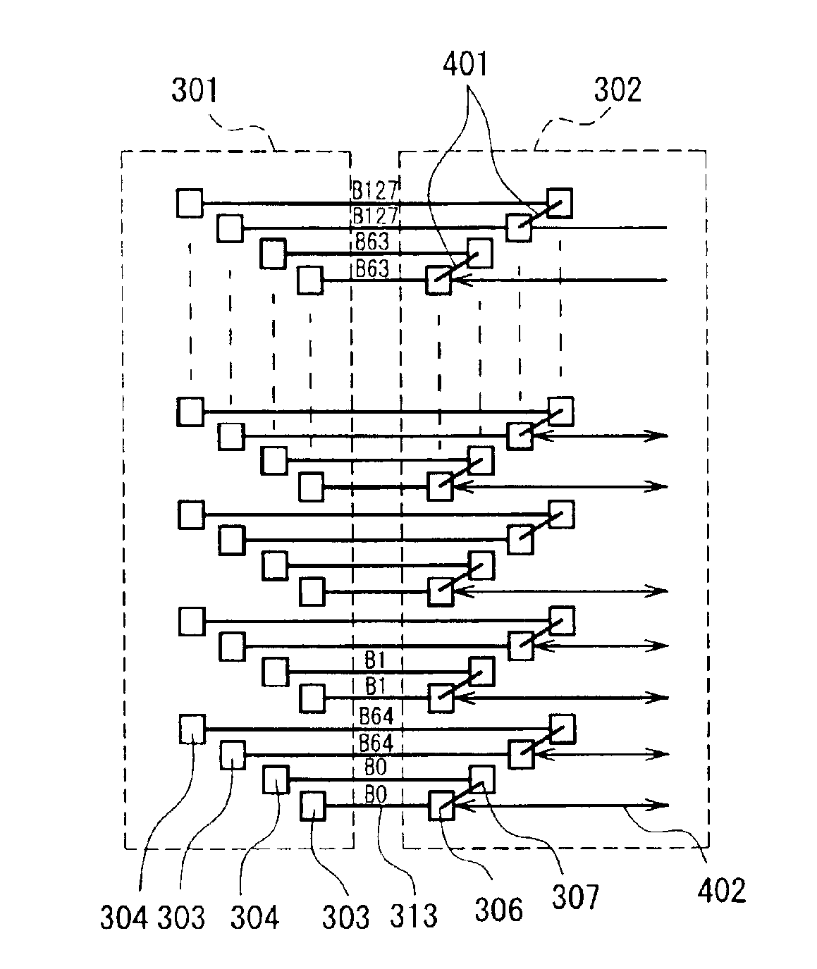
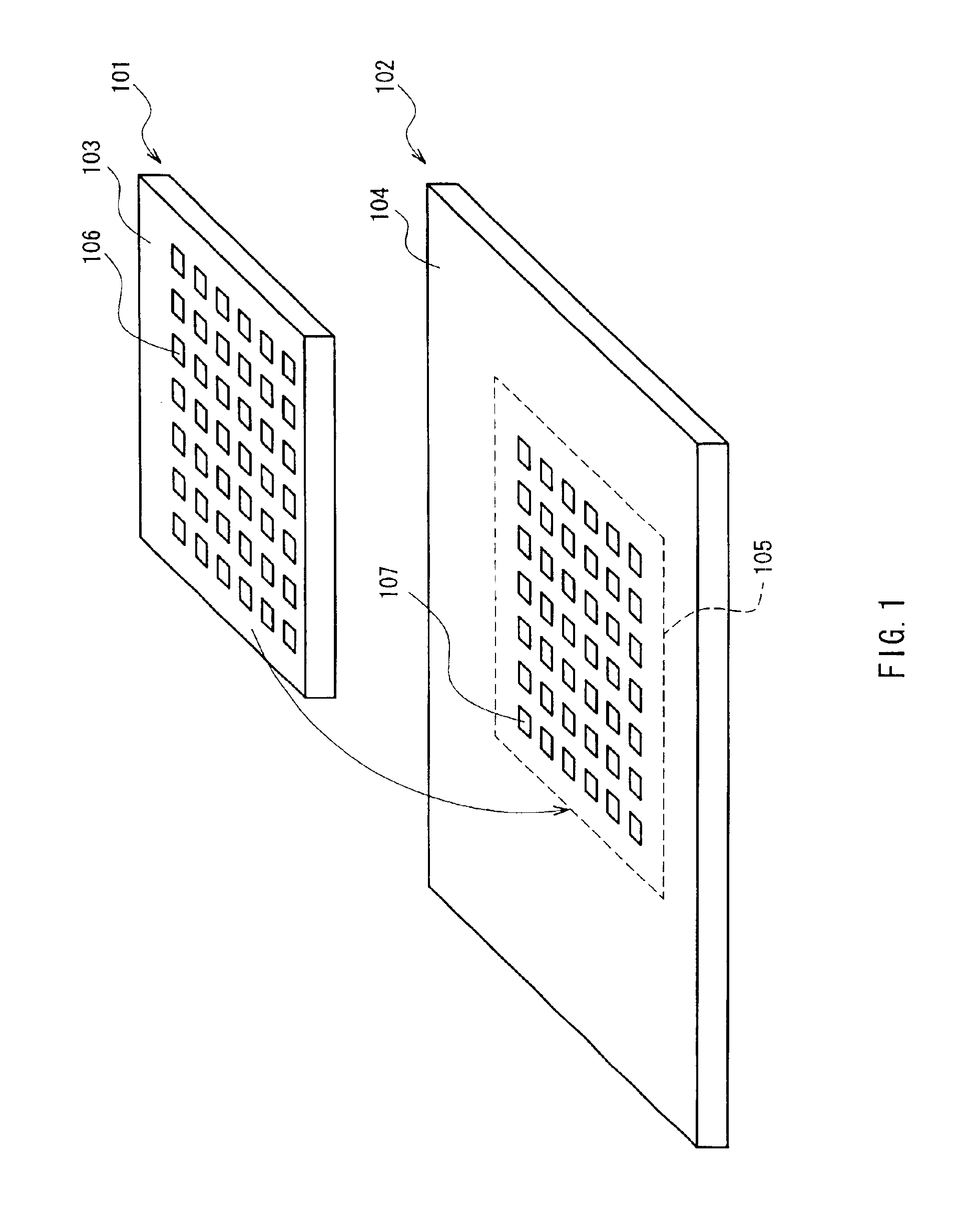
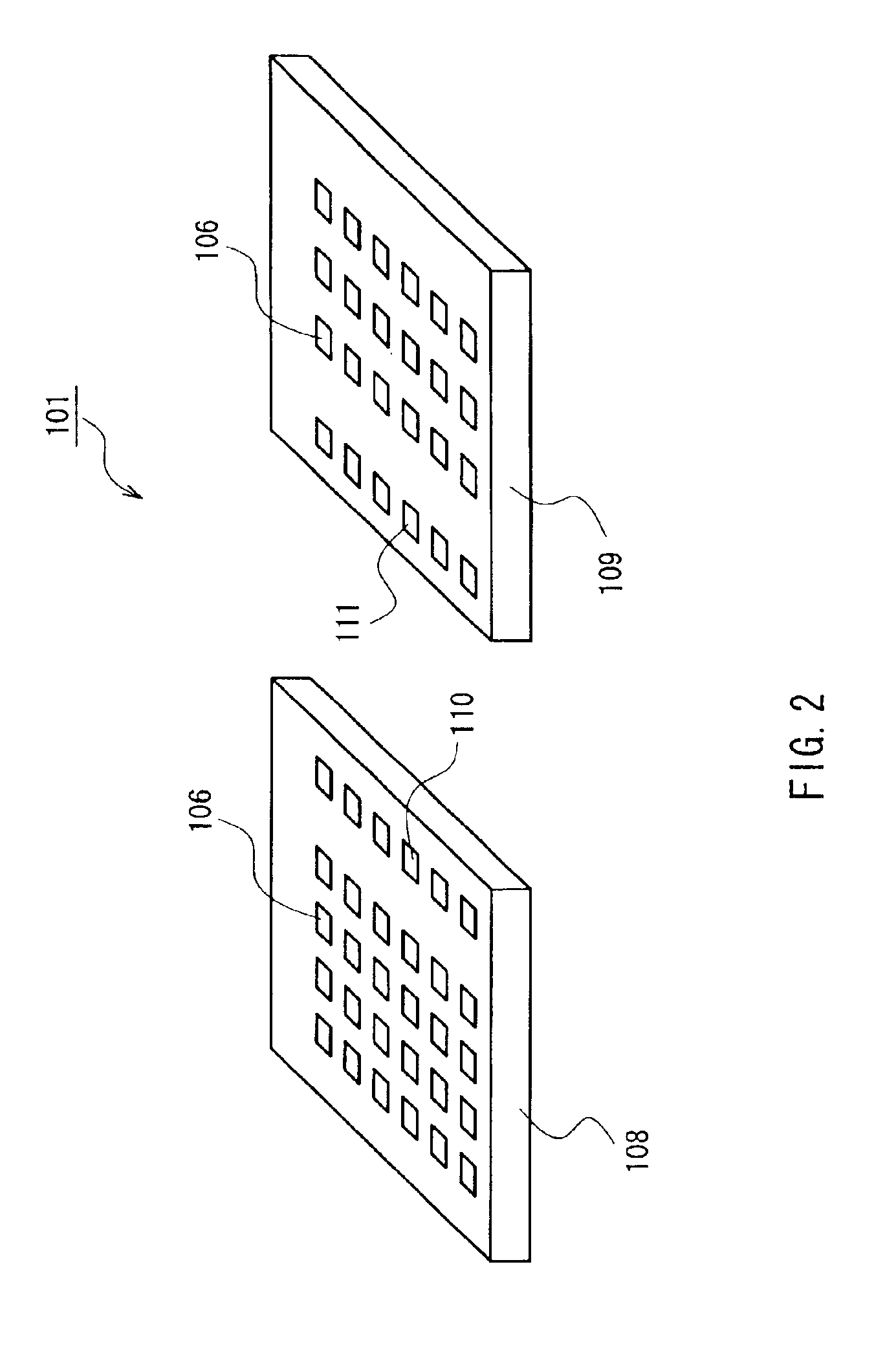
FIG. 1 is a schematic view illustrating a state of bonding a semiconductor memory device according to an embodiment of the present invention to another semiconductor device. In FIG. 1, numeral 101 denotes a semiconductor memory device composed of a single silicon chip. Numeral 102 denotes another semiconductor device such as a logic LSI or the like. Numeral 103 denotes a surface on which functional elements, bonding bumps of the semiconductor memory device 101 are formed. Numeral 104 denotes a surface on which functional elements, bonding bumps of another semiconductor device 102 are formed. Numeral 105 denotes a bonding area. Numerals 106 and 107 denote bonding bumps. The semiconductor memory device 101 composed of a single silicon chip is connected to the bonding area 105 of another semiconductor device 102 by stacking the bonding bumps 106 and 107 on one another.

It should...


PUM


Abstract

A semiconductor memory device for use in a semiconductor device with a chip on chip structure, which enables a memory specification to be selected and fixed, and improves design and production efficiencies. Bonding bumps corresponding to an input terminal and an output terminal of an interface circuit are connected to bonding bumps provided on another semiconductor device. Then, a polarity of a potential on a bus width varying terminal is fixed by the bonding bump provided on another semiconductor device, so that an isolated input / output specification is selected as a bus specification of the interface circuit and a bus width is selected.

Description

FIELD OF THE INVENTIONThe present invention relates to a semiconductor memory device, such as a dynamic random access memory (DRAM) and a flash memory, for use in a semiconductor device with a so-called chip on chip (COC) structure.BACKGROUND OF THE INVENTIONConventionally, the following two structures have been adopted to provide a so-called system LSI on which a memory with a large capacity equal to or more than several M bits mainly is mounted: a single chip structure according to an embedded memory process, in which a logic and a memory are integrated into a single chip; or a single package structure according to a stack structure, in which a logic LSI and a memory LSI are integrated into a single package.Since the single chip structure according to the embedded memory process allows a logic and a memory on the common semiconductor chip to be connected by a multi-bit bus, a high transfer rate and low power consumption can be realized, and a memory specification can be varied eas...

Claims


Application Information

Patent Timeline
Patent Type & Authority Patents(United States)
IPC IPC(8): G11C16/02G11C11/401H01L25/065H01L21/70H01L21/44H01L23/16H01L21/336H01L23/48H01L21/02H01L21/8234H01L25/07H01L25/18
CPCH01L25/0657H01L25/18H01L2225/06513H01L2225/06527H01L2924/0002H01L2924/00
Inventor NAKAI, NOBUYUKI
Owner CETUS TECH INC
Why Eureka
Try Eureka