Multi-chips stacked package

a technology of stacking and chips, applied in the field of stacking packages, can solve the problems of reducing affecting the development of packaged integrated circuits of higher performance, and affecting the development speed of integrated circuits, so as to prevent the damage of the upper chip

Inactive Publication Date: 2007-08-02
ADVANCED SEMICON ENG INC
View PDF9 Cites 7 Cited by
  • Summary
  • Abstract
  • Description
  • Claims
  • Application Information

AI Technical Summary

Benefits of technology

[0009] In view of the above-mentioned problems, an objective of this invention is to provide a multi-chips stacked package to improve the reliability of the wire-bonding process and prevent the upper chip from being easily damaged and cracked. Therein, a carrier is provided on the lower chips to carry the upper chip so as to prevent the upper chip from being directly disposed on the lower chips and to solve the above-mentioned disadvantage.
[0011] As mentioned above, the carrier may be a printed circuits board (PCB). Generally speaking, the carrier comprises a core layer and a copper layer. Therein the copper layer can be a circuit layer and is regarded as electrical paths for transmitting electrical signals. The core layer can be made of Bismaleimide-Triazine (BT) or glass epoxy resins (FR-4) so that the carrier is able to bear the wire-bonding force by the stiffness of the core layer in the performance of the wire-bonding process. Thus, the upper chip can be prevented from damaging.

Problems solved by technology

Recently, integrated circuit (chip) packaging technology is becoming a limiting factor for the development in packaged integrated circuits of higher performance.
Semiconductor package designers are struggling to keep pace with the increase in pin count, size limitations, low profile, and other evolving requirements for packaging and mounting integrated circuits.
Thus, the upper chips 12 and 13 will be damaged and cracked more easily in the operation of the wire-bonging process.
However, when the distance between the lower chips 22 and 23 is larger than 50 μm, the portion 242 of the lower surface of the upper chip 24 not supported by the lower chips 22 and 23 will be damaged easily in the performance of the wire-bonding process.

Method used


Image

  • Multi-chips stacked package
  • Multi-chips stacked package
  • Multi-chips stacked package

Examples


second embodiment

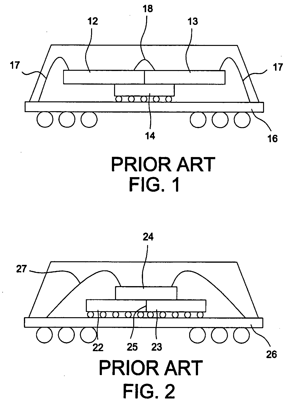
[0024] Besides, as shown in FIG. 5, it illustrates a second embodiment in according to this invention. The upper chip 34 is mounted on the carrier 35 via a plurality of electrically conductive bumps 342, for example solder bumps and gold bumps. In addition, the carrier 35 further has a circuit layer 352 for electrically connecting to the electrically conductive bumps 342. Thus, the upper chip 34 is electrically connected to the first lower chip 32 and the second lower chip 33 through the electrically conductive bumps 342, the circuit layer 352 and the electrically conductive wires 38.

[0025] Furthermore, as shown in FIG. 6, it illustrates a third preferred embodiment according to this invention. The upper chip 34 is electrically connected to the carrier 35 via a plurality of electrically conductive bumps 342 and the upper chip 34 is electrically connected to the substrate 36 through the electrically conductive bumps 342, the circuit layer 352 and electrically conductive wires 38′.

fourth embodiment

[0026] Next, as shown in FIG. 7, it illustrates a The upper chip 34 is electrically connected to the carrier 35 via a plurality of electrically conductive wires 39 by wire-bonding technology. Similarly, the carrier 35 further comprises a circuit layer 352 so as to have the upper chip 34 electrically connected to the substrate 36 through the electrically conductive wires 39, the circuit layer 352 and another electrically conductive wires 38″.

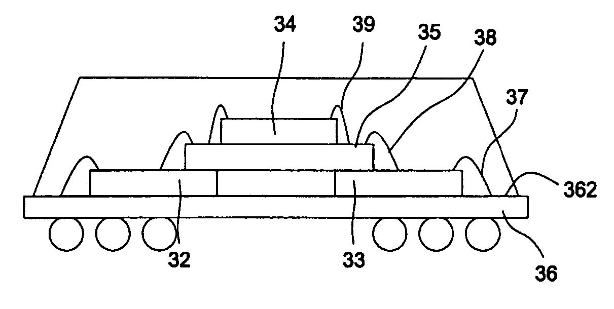
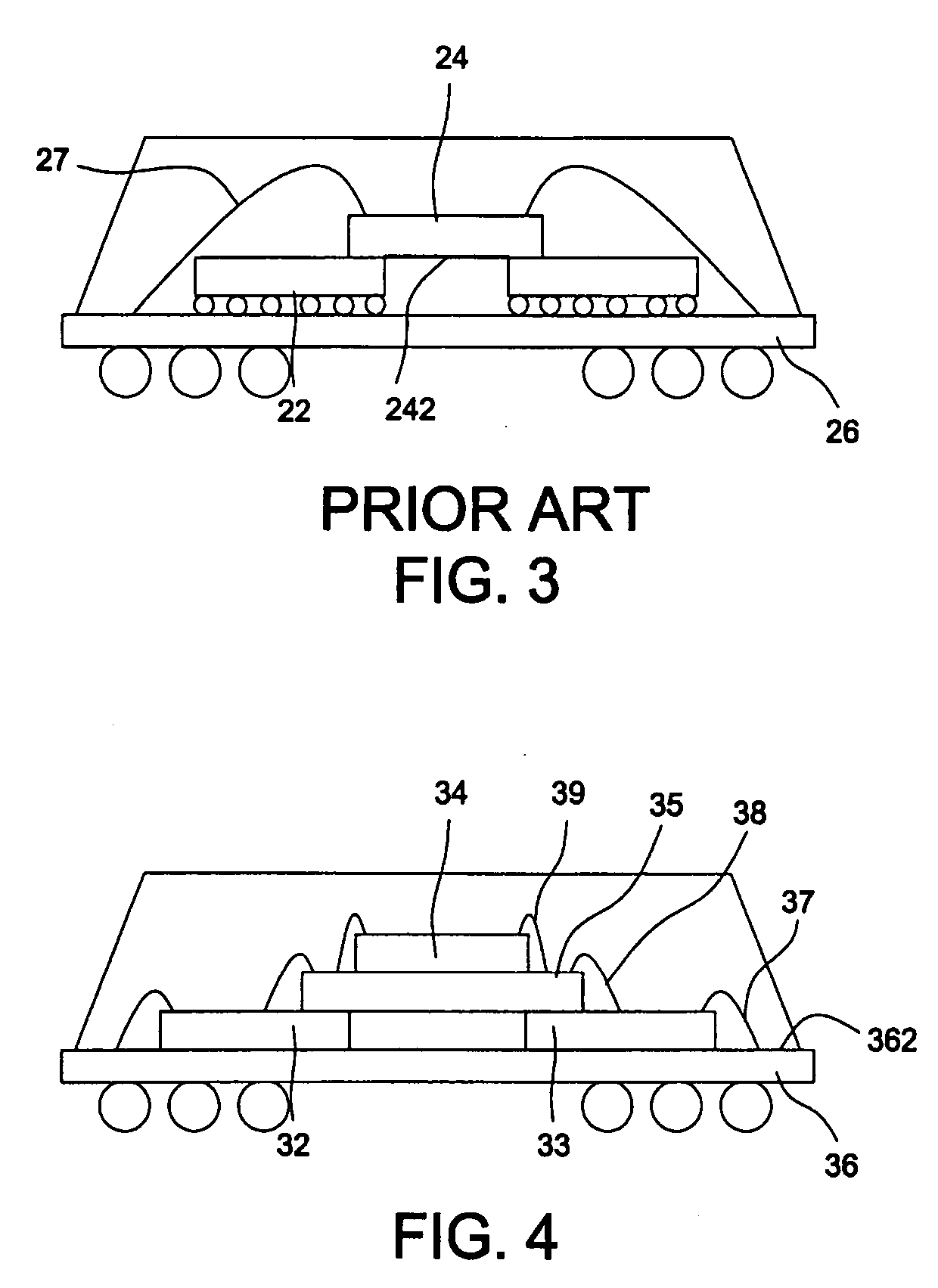
[0027] As mentioned above, said carrier 35 can be a printed circuit board. Generally speaking, it is composed of a core layer and a copper layer. Therein, the copper layer is patterned to form a circuit layer to be electrical paths and the core layer is formed of a material selected from Bismaleimide-Triazine (BT) and glass epoxy resins (FR4) so that the carrier 35 is able to bear the wire-bonding force by the stiffness of the core layer in the performance of the wire bonding process. Thus, the upper chip 34 can be prevented from being damaged. ...

sixth embodiment

[0029] Finally, referring to FIG. 9, there is provided a Said first lower chip 42 and said second lower chip 43 are disposed on the upper surface 462 of the substrate 46, and electrically connected to the substrate 46 via electrically conductive wires 48. In addition, the carrier 45 is disposed on the first lower chip 42 and the second lower chip 43 simultaneously, and electrically connected to the first lower chip 42 and the second lower chip 43 through electrically conductive bumps 47. Moreover, the upper chip 44 is disposed on the carrier 45 and electrically connected to the first lower chip 42 and the second lower chip 43 through electrically conductive wires 49, a circuit layer 452, a plurality of electrically conductive bumps 47. After the electrical signals are transmitted from the upper chip 44 to the first lower chip 42 and the second lower chip 43, the signals will be transmitted to the substrate 46 through electrically conductive wires 48. It should be noted that the ref...


PUM


Abstract

A multi-chips stacked package mainly comprises a substrate, a first lower chip, a second lower chip, an upper chip and a carrier. The substrate has an upper surface, and the first lower chip and the second lower chip are disposed on the upper surface of the substrate and electrically connected to the substrate. The carrier is disposed on and electrically connected to the first lower chip and the second lower chip simultaneously, and the upper chip is mounted on the carrier. Moreover, the upper chip is electrically connected to the substrate through the carrier, the first lower chip or the second lower chip.

Description

BACKGROUND OF THE INVENTION [0001] 1. Field of Invention [0002] This invention relates to a multi-chips stacked package. More particularly, the present invention is related to a multi-chips stacked package having a carrier for carrying the upper chip for preventing the upper chip from being directly disposed on the lower chip. [0003] 2. Related Art [0004] Recently, integrated circuit (chip) packaging technology is becoming a limiting factor for the development in packaged integrated circuits of higher performance. Semiconductor package designers are struggling to keep pace with the increase in pin count, size limitations, low profile, and other evolving requirements for packaging and mounting integrated circuits. [0005] Due to the assembly package in miniature and the integrated circuits operation in high frequency, MCM (multi-chips module) packages are commonly used in said assembly packages and electronic devices. Usually, said MCM package mainly comprises at least two chips encap...

Claims


Application Information

Patent Timeline
Patent Type & Authority Applications(United States)
IPC IPC(8): H01L23/02H01L25/065
CPCH01L25/0652H01L2224/16H01L2224/32145H01L2224/48091H01L2224/48227H01L2924/01087H01L2225/06562H01L2924/01079H01L2924/15311H01L2224/73207H01L2924/00014H01L2224/16225H01L2924/19107H01L2224/73265H01L2224/0401H01L2924/00
Inventor WANG, SUNG-FEI
Owner ADVANCED SEMICON ENG INC
Why Eureka
Try Eureka