Semiconductor device for radio communication device, and radio communication device using said semiconductor device

a technology of semiconductor devices and radio communication devices, which is applied in the direction of electrical apparatus construction details, multi-frequency-changing modulation transference, transmission, etc., can solve the problems of lengthening the lifetime of the incorporated battery of a mobile phone or the like, and achieve the effect of reducing losses in inter-chip wiring and simplifying arrangemen

Inactive Publication Date: 2006-08-08
TAIWAN SEMICON MFG CO LTD
View PDF18 Cites 7 Cited by
  • Summary
  • Abstract
  • Description
  • Claims
  • Application Information

AI Technical Summary

Benefits of technology

[0015]It is an object of the present invention to provide a semiconductor device for a radio communication device, of which arrangement can be simplified and in which the losses in the inter-chip wirings can be reduced, and also to provide a radio communication device using such a semiconductor device.

Problems solved by technology

This lengthens the lifetime of the incorporated battery of a mobile phone or the like.

Method used


Image

  • Semiconductor device for radio communication device, and radio communication device using said semiconductor device
  • Semiconductor device for radio communication device, and radio communication device using said semiconductor device
  • Semiconductor device for radio communication device, and radio communication device using said semiconductor device

Examples


Embodiment Construction

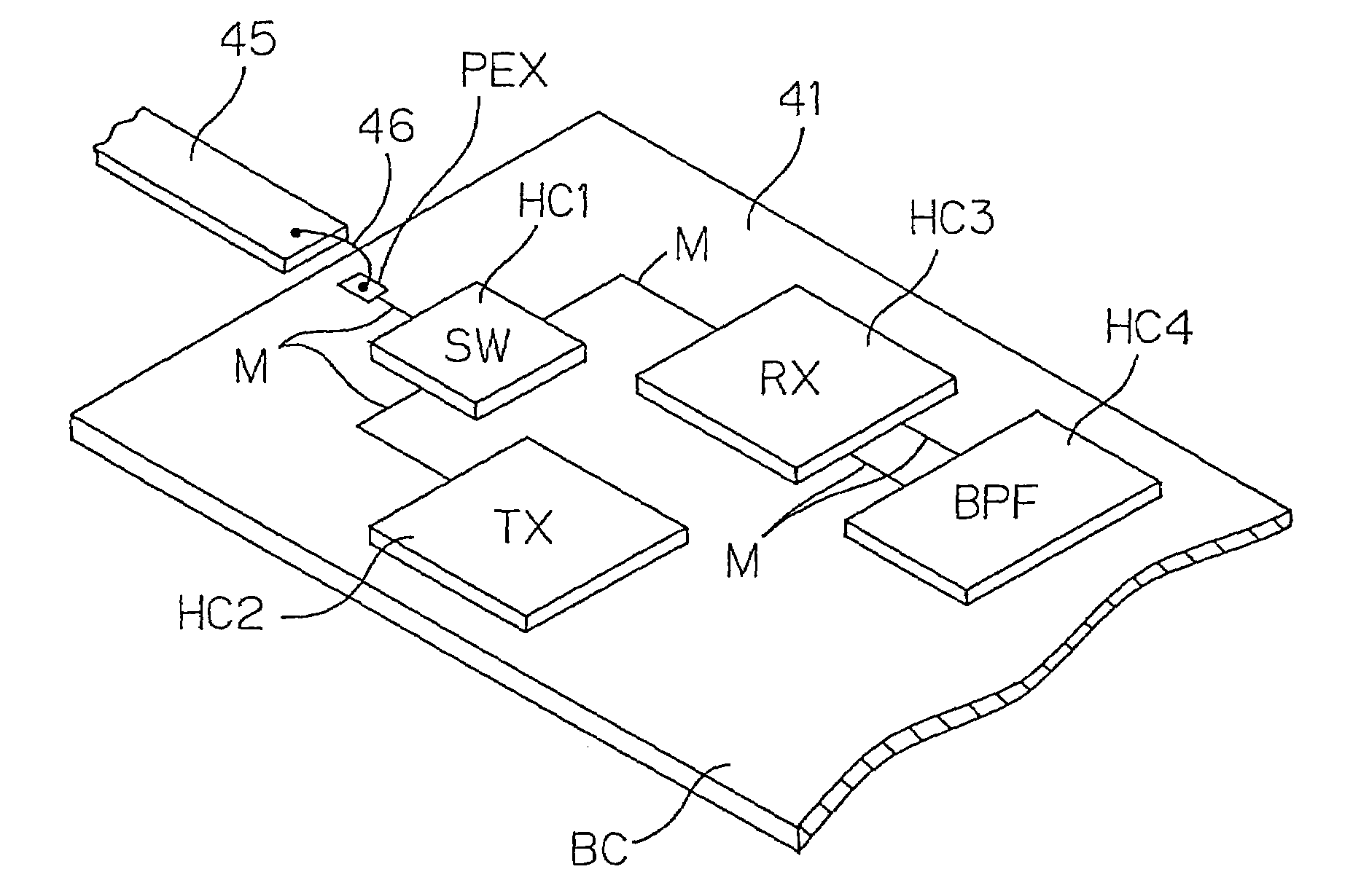
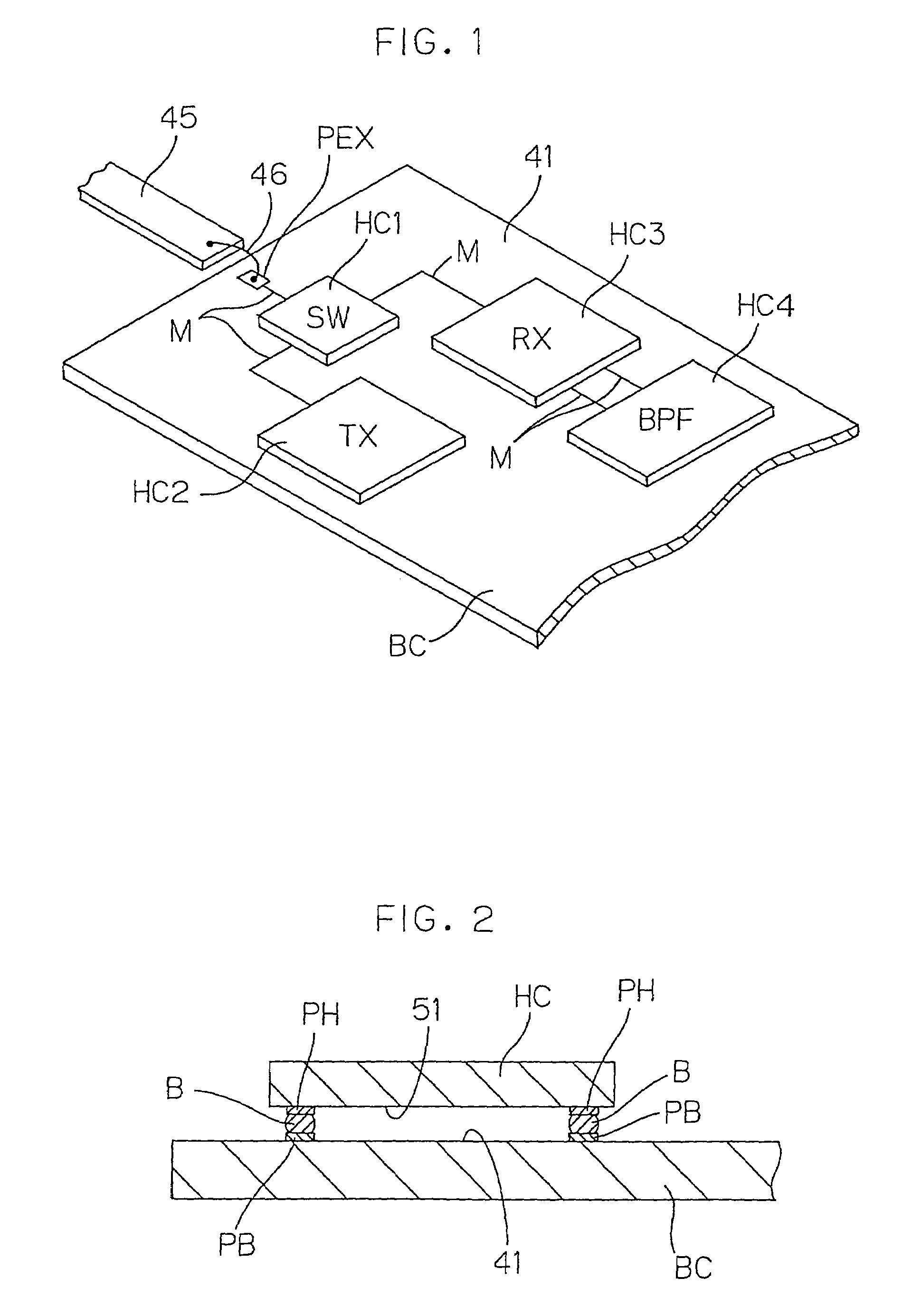
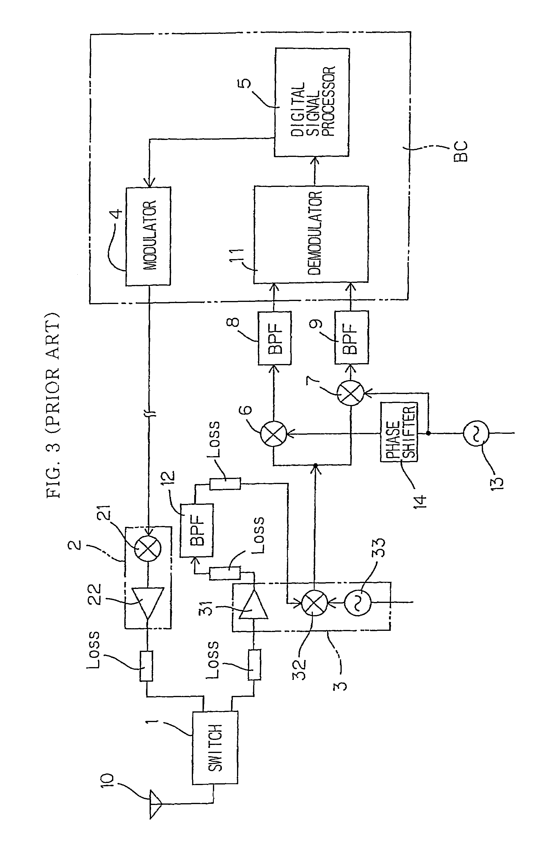
[0034]FIG. 1 is a perspective view illustrating the arrangement of a semiconductor device forming the transmitter / receiver units and the like of a mobile phone, according to an embodiment of the present invention. The electric arrangement of the mobile phone according to this embodiment, is the same as that shown in FIG. 3. Accordingly, to avoid a repeated explanation, the following description will be made with reference to FIG. 3.

[0035]This embodiment provides a chip-on-chip-structure semiconductor device in which a plurality of high-frequency chips HC1, HC2, HC3, HC4, . . . (hereinafter referred to as “high-frequency chips HC” when these chips are collectively referred to) are piled upon and bonded to, with the surfaces down, the surface 41 of a base band chip BC.

[0036]The base band chip BC is formed by a silicon semiconductor chip in which integrated are a modulator unit 4, a digital signal processing unit 5 and a demodulator unit 11. The high-frequency chip HC1 is formed by a g...


PUM


Abstract

A chip-on-chip-structure semiconductor device for a radio communication device, having a base band chip and a high-frequency chip piled up on and bonded to the surface thereof. The base band chip has a low-frequency signal processing unit for processing a signal in a first frequency band. The high-frequency chip has a high-frequency signal processing unit for processing a signal in a second frequency band of which frequency is higher than that of the first frequency band.

Description

[0001]This application is a continuation Application of Ser. No. 09 / 493,251 filed Jan. 28, 2000 now abandoned.BACKGROUND OF THE INVENTION[0002]1. Field of the Invention[0003]The present invention relates to a semiconductor device to be applied for a radio communication device such as a mobile phone or the like, and also to a radio communication device using said semiconductor device.[0004]2. Description of Related Art[0005]FIG. 3 is a block diagram illustrating the electric arrangement of a mobile phone of which typical examples include a vehicle phone and a portable phone. An antenna 10 for transmitting and receiving a radio signal, is connected to a switch unit 1 for separating a transmission signal and a reception signal from each other. Connected to this switch unit 1 are a transmitter unit 2 and a receiver unit 3. A signal from a digital signal processing unit 5 (signal processing unit) is given to the transmitter unit 2 through a suitable filter circuit (not shown) after modul...

Claims


Application Information

Patent Timeline
Patent Type & Authority Patents(United States)
IPC IPC(8): H04B1/28H01L25/00H01L25/065H01L25/07H01L25/18H04B1/38
CPCH04B1/3833H01L2924/19107H01L2224/16225H01L2224/05568H01L2224/05573H01L2924/00014H01L2224/05599
Inventor HIKITA, JUNICHIMOCHIDA, HIROONAGI, KATSUTOSHI
Owner TAIWAN SEMICON MFG CO LTD
Why Eureka
Try Eureka