Method for shaping table surface of semiconductor chip

A semiconductor and chip technology, applied in the field of semiconductor chip production, can solve the problems of poor coordination, rough cutting surface, scrapped devices, etc., and achieve the effects of fine angle matching, improved efficiency, and avoiding edge collapse

Inactive Publication Date: 2015-09-30
ZHUZHOU CSR TIMES ELECTRIC CO LTD
View PDF8 Cites 6 Cited by
  • Summary
  • Abstract
  • Description
  • Claims
  • Application Information

AI Technical Summary

Problems solved by technology

[0006] (1) Due to the problem of the processing direction, the traditional mechanical grinding method cannot process the double positive angle table shape (the end face is dovetail shape);
[0007] (2) The efficiency is low, only one surface of the chip 2 can be ground at one angle at a time, and the grinding disc 1 needs to be replaced every time the grinding of one angle is completed;
[0008] (3) Since the grinding of each angle is independent of each other, the risk is that the coordination effect designed by eac

Method used


Image

  • Method for shaping table surface of semiconductor chip
  • Method for shaping table surface of semiconductor chip
  • Method for shaping table surface of semiconductor chip

Examples


Embodiment Construction

[0035] The present invention will be further described in detail below in conjunction with the accompanying drawings and specific embodiments.

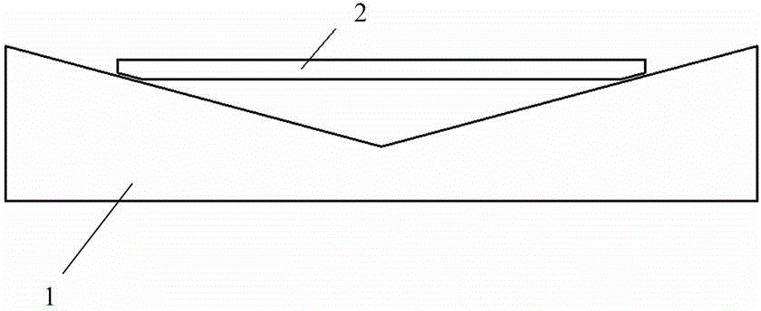
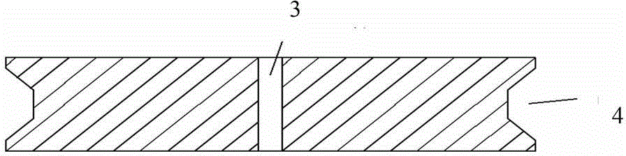
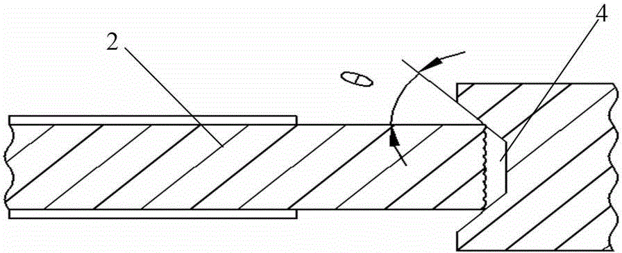
[0036] A kind of semiconductor chip mesa modeling method of the present invention, uses the circular grinding wheel 3 of high-speed rotation, offers the groove 4 corresponding to required groove type on the grinding wheel 3, is plated with diamond in the groove 4, puts on the chip 2 to be processed The cylindrical surface of the chip junction terminal extends into the groove 4, and forms the table top by contacting the groove 4, which can simultaneously shape the double-sided multi-angle, the angle is finely matched, and the efficiency is greatly improved. In this way, when the bevel grinding is performed on the chip 2, the rough end surface produced by cutting the circle is also ground at the same time, so as to avoid chipping and splitting at the edge, and the improvement of the edge condition is conducive to improving the reliabilit...


PUM

PropertyMeasurementUnit
Chamferaaaaaaaaaa

Abstract

The invention discloses a method for shaping the table surface of a semiconductor chip. The method comprises the following steps: using a grinding wheel rotating at a high speed, forming a groove corresponding to the needed groove shape in the grinding wheel, plating a grinding layer in the groove, and after the cylindrical surface of a chip ending terminal on the chip to be machined stretches in the groove, shaping the table surface by means of contacting with the groove and grinding. The method disclosed by the invention has the advantages of being convenient and efficient, simple in process, high in yield, low in manufacturing cost, and the like.

Description

technical field [0001] The invention mainly relates to the manufacturing field of semiconductor chips, in particular to a mesa modeling method suitable for semiconductor chips. Background technique [0002] In high-voltage power semiconductor devices, the reverse withstand voltage of the PN junction usually does not meet the design requirements, the main reason is that surface breakdown occurs. In order to reduce the adverse effects of surface effects and thereby improve the blocking capability of planar semiconductor devices, it is usually necessary to treat the junction terminals of the devices. [0003] So far, many high-voltage junction termination technologies have been developed, such as field limiting ring method (FLR), field plate method (FP), mesa (bevel) molding method, corrosion molding method, junction termination extension method, semi-insulating polysilicon technology (SIPOS ), junction termination extension technology (JTE), weakened surface electric field te...

Claims


Application Information

Patent Timeline
IPC IPC(8): H01L21/304
CPCH01L21/304
Inventor 操国宏吴煜东刘锐鸣邹冰艳颜骥
Owner ZHUZHOU CSR TIMES ELECTRIC CO LTD
Why Eureka
Try Eureka