LED device having improved power distribution

a technology of led devices and power distribution, which is applied in the direction of discharge tubes/lamp details, organic semiconductor devices, discharge tubes/lights, etc., can solve the problems of difficult fabrication of masks, difficult to fabricate expensive metal shadow masks, and difficult to clean and replace masks

Active Publication Date: 2009-07-23
GLOBAL OLED TECH
View PDF9 Cites 43 Cited by
  • Summary
  • Abstract
  • Description
  • Claims
  • Application Information

AI Technical Summary

Benefits of technology

[0013]The aforementioned need is addressed according to the present invention by providing an LED device that includes electrodes patterned over a substrate; the pattern forming several first electrodes separated by inter-electrode spacers. One or more light-emitting layers are formed over the first electrodes. A patterned conductive layer is formed over the one or more li...

Problems solved by technology

For small-molecule organic materials, such patterned deposition is done by evaporation and is quite difficult, requiring, for example, expensive metal shadow-masks.
These masks are difficult to fabricate and must be cleaned and replaced frequently.
Material deposited on the mask in prior manufacturing cycles may flake off and cause particulate contamination.
Moreover, aligning shadow-masks with a substrate is problematic and often damages the materials already deposited on the substrate.
Further, the masks are subject to thermal expansion during the organic LED material deposition process, reducing the deposition precision and limiting the resolution and size at which the pattern may be formed.
However, this method creates significant particulate contamination that can deleteriously affect subsequent processing steps, for example, the deposition of materials or encapsulation of a device.
In either of these cases, the subsequent location of a mask ...

Method used


Image

  • LED device having improved power distribution
  • LED device having improved power distribution
  • LED device having improved power distribution

Examples


Embodiment Construction

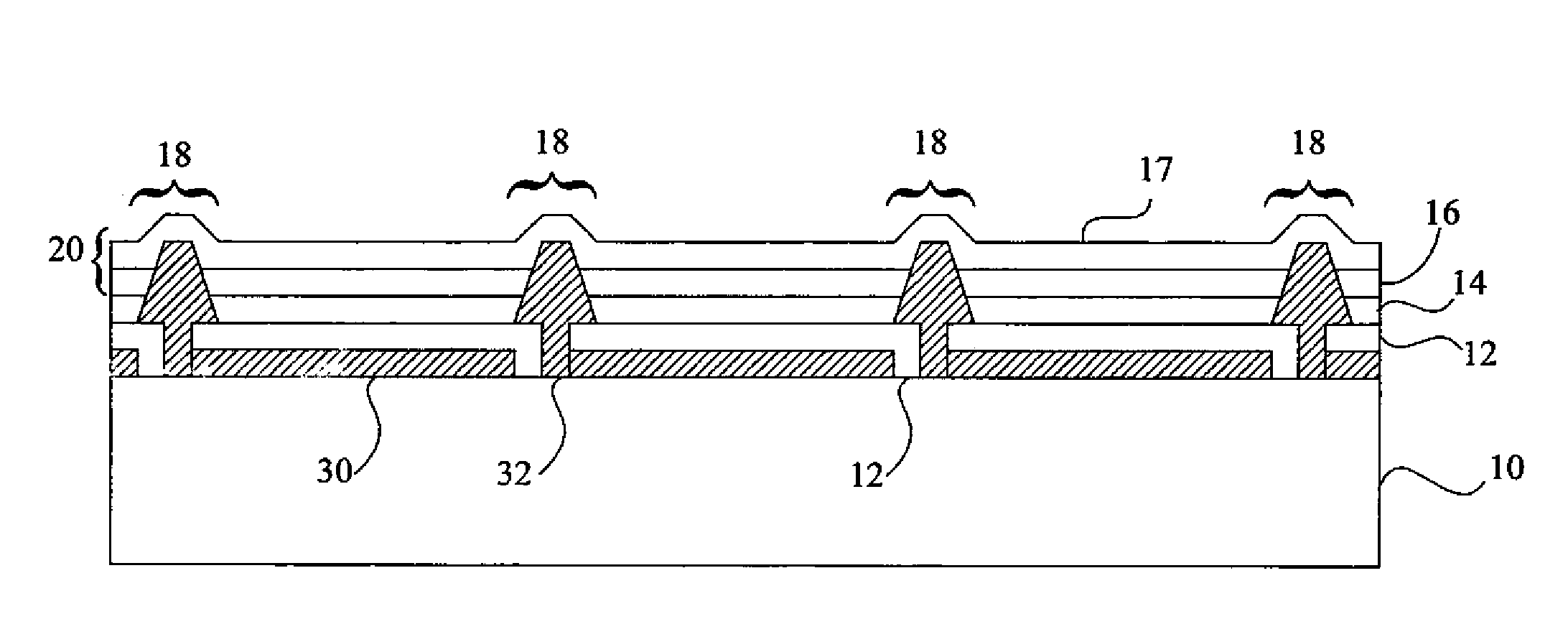
[0028]Referring to FIG. 1, in one embodiment of the present invention, an LED device comprises a substrate 10 on which is formed a plurality of laterally-spaced electrodes patterned over the substrate 10, the pattern forming a plurality of first electrodes 12 separated by inter-electrode spacers 18. One or more light-emitting layers 14 are formed over the plurality of first electrodes 12, and a patterned conductive layer 16 is formed over the one or more light-emitting layers 14 and over the plurality of first electrodes 12, in regions external to the inter-electrode spacers 18. A continuous unpatterned conductive layer 17 is formed over both the patterned conductive layer 16 and the inter-electrode spacers 18, wherein a combination of the patterned and continuous unpatterned conductive layers 16, 17 form a single, bi-layered electrically continuous second electrode 20. By regions external to the inter-electrode spacers 18 is meant that the materials forming the patterned conductive...


PUM


Abstract

An LED device that includes electrodes patterned over a substrate; the pattern forming several first electrodes separated by inter-electrode spacers. One or more light-emitting layers are formed over the first electrodes. A patterned conductive layer is formed over the one or more light-emitting layers and over the first electrodes in regions external to the inter-electrode spacers. A continuous unpatterned conductive layer is formed over both the patterned conductive layer and the inter-electrode spacers. Finally, a combination of the patterned and continuous unpatterned conductive layers form a single, bi-layered, electrically continuous second electrode.

Description

FIELD OF THE INVENTION[0001]The present invention relates to top-emitting light-emitting diode (LED) devices and, more particularly, to an LED device having improved manufacturing yields and power distribution in an upper electrode, and a method of making thereofBACKGROUND OF THE INVENTION[0002]Light-emitting diode (LED) devices, also referred to as electroluminescent (EL) devices, have numerous well-known advantages over other flat-panel display devices currently in the market place. Among these advantages are brightness of light emission, relatively wide viewing angle, and reduced electrical power consumption compared to, for example, liquid crystal displays (LCDs) using backlighting. Such devices may be made with light-emitting layers comprising organic materials or inorganic materials such as quantum dots.[0003]Applications of LED devices include active-matrix image displays, passive-matrix image displays, and area-lighting devices such as, for example, selective desktop lightin...

Claims


Application Information

Patent Timeline
IPC IPC(8): H01J1/62B05D5/12
CPCH01L27/3246H01L27/3283H01L2251/5315H01L51/56H01L51/5234H10K59/173H10K59/122H10K50/828H10K2102/3026H10K71/00
Inventor COK, RONALD S.
Owner GLOBAL OLED TECH
Why Eureka
Try Eureka