Flip chip quad flat non-leaded package structure and manufacturing method thereof and chip package structure

Inactive Publication Date: 2009-07-30
CHIPMOS TECH INC
View PDF4 Cites 16 Cited by
  • Summary
  • Abstract
  • Description
  • Claims
  • Application Information

AI Technical Summary

Benefits of technology

[0011]The present invention is directed to a manufacturing method of a flip chip quad flat non-leaded package

Problems solved by technology

However, the QFN type is high-cost and bulky.
Besides, the chip pads of the conventional QFN packages are electrically and directly connected to the leads via bumps, and therefore the size of the flip chip QFN package structures are sure to the size of the leads of the lead frame, and i

Method used


Image

  • Flip chip quad flat non-leaded package structure and manufacturing method thereof and chip package structure
  • Flip chip quad flat non-leaded package structure and manufacturing method thereof and chip package structure
  • Flip chip quad flat non-leaded package structure and manufacturing method thereof and chip package structure

Examples


Embodiment Construction

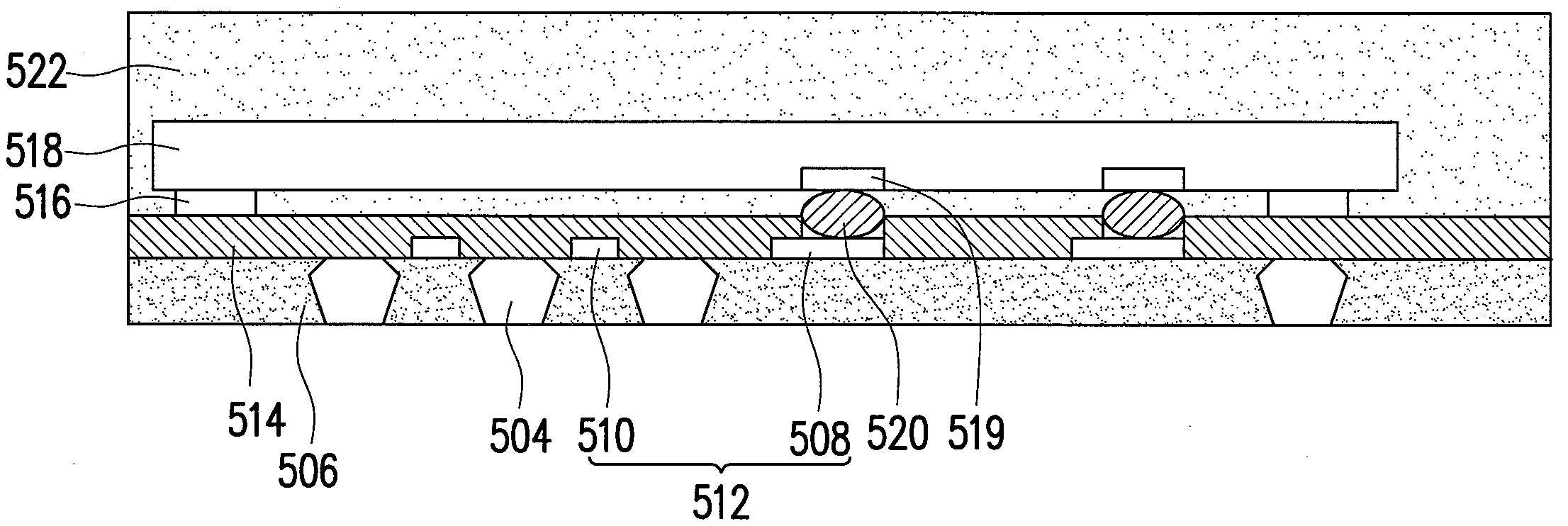
[0056]Reference will now be made in detail to the present preferred embodiments of the invention, examples of which are illustrated in the accompanying drawings. Wherever possible, the same reference numbers are used in the drawings and the description to refer to the same or like parts.

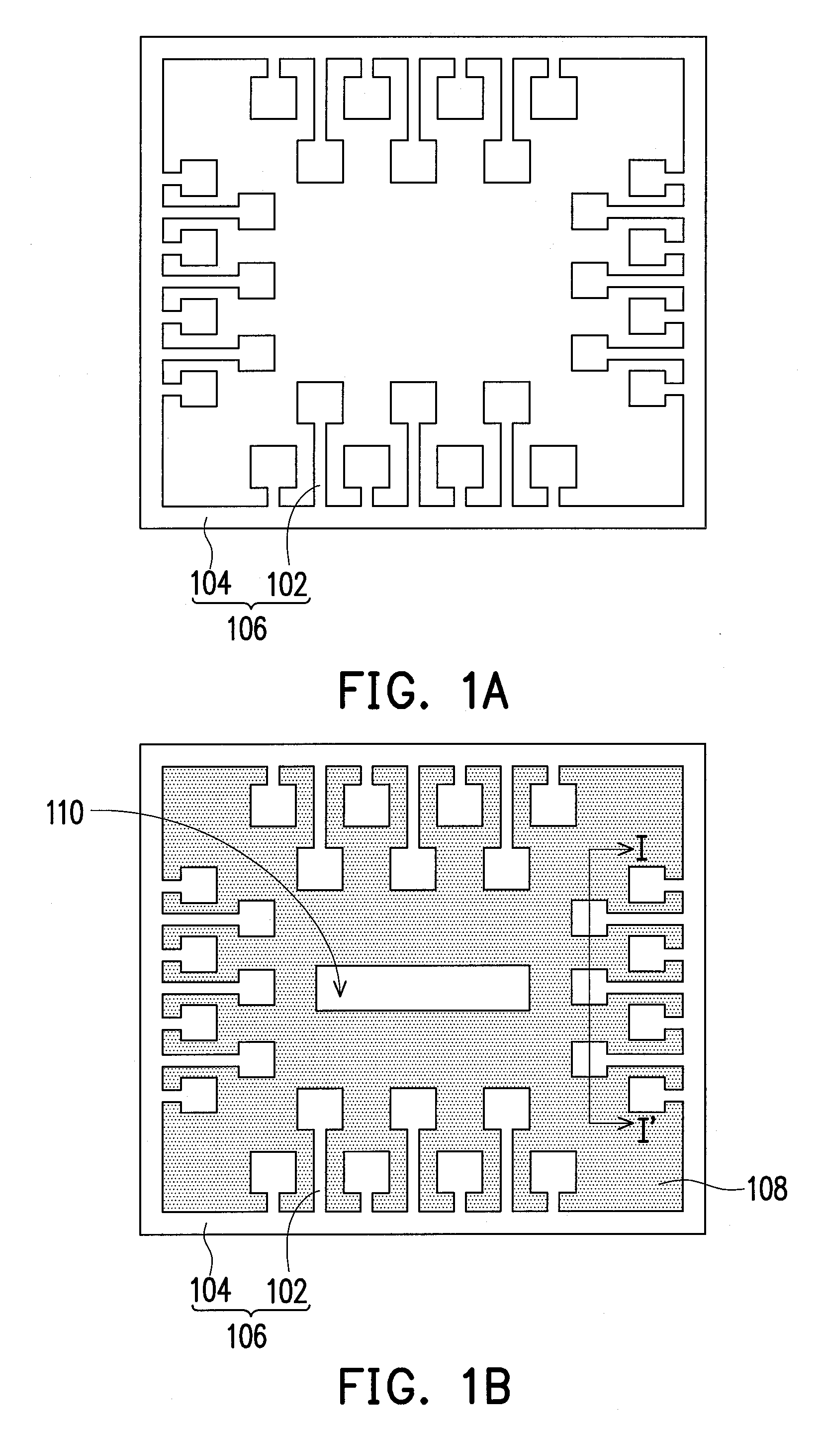
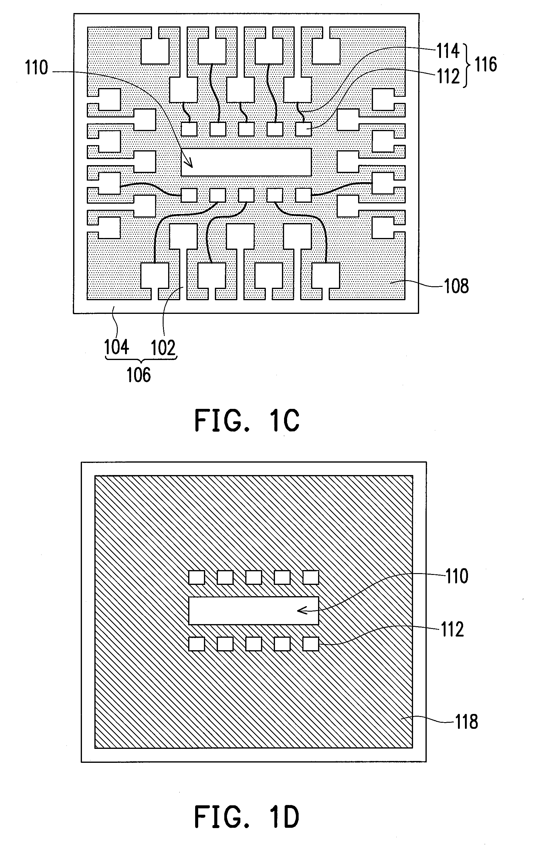
[0057]FIGS. 1A through 1F are schematic cross-sectional views illustrating a manufacturing method of a flip chip quad flat non-leaded package structure according to an embodiment of the present invention.

[0058]As shown in FIG. 1A, in a manufacturing method of a flip chip quad flat non-leaded package structure according to the present embodiment, which includes the following steps. A lead frame 106 having a plurality of lead 102 is provided at first. In the present embodiment, the lead frame 106 further includes a frame 104. The leads 102 of the lead frame 106 are connected with the frame 104 and arranged along the center of the frame 104 and extending to an array or a single row (not shown). For inst...


PUM


Abstract

A manufacturing method for a Flip Chip Quad Flat Non-leaded package structure is provided. A lead frame having a plurality of leads is provided at first in the manufacturing method. A dielectric layer is formed on the lead frame and exposes a top surface and a bottom surface of the leads. A redistribution layer including a plurality of pads and a plurality of conductive lines connected the pads and the top surface of the leads is formed on the dielectric layer. A solder resist layer is formed to cover the redistribution layer, the dielectric layer and the leads, and expose the surface of the pads. An adhesive layer is formed on the solder resist layer. A chip having a plurality of bumps is provided. The chip is adhered on the solder resist layer with the adhesive layer and each bump is electrically connected with one of the pads.

Description

CROSS-REFERENCE TO RELATED APPLICATION[0001]This application claims the priority benefits of Taiwan applications of serial no. 97103472, filed on Jan. 30, 2008, serial no. 97103470, filed on Jan. 30, 2008 and serial no. 97105932, filed on Feb. 20, 2008. The entirety of each of the above-mentioned patent applications is hereby incorporated by reference herein and made a part of this specification.BACKGROUND OF THE INVENTION[0002]1. Field of the Invention[0003]The present invention generally relates to a package structure and a manufacturing method thereof. More particularly, the present invention relates to a flip chip quad flat non-leaded (QFN) package structure and manufacturing method thereof, and a chip package structure for enhancing the efficiency of the devices.[0004]2. Description of Related Art[0005]In semiconductor industry, production of integrated circuit (IC) is mainly divided into three stages: IC design, IC process and IC package. The package may prevent the chip from ...

Claims


Application Information

Patent Timeline
IPC IPC(8): H01L23/52H01L21/00
CPCH01L23/3114H01L23/49517H01L23/49822H01L2924/01079H01L2224/16H01L2924/01078H01L23/49861H01L2224/05571H01L2224/05573H01L2224/0615H01L2924/00014H01L2924/181H01L2224/05599H01L2924/00012
Inventor WU, CHENG-TINGLIN, HUNG-TSUNCHEN, YU-RENLIN, CHUN-YING
Owner CHIPMOS TECH INC
Why Eureka
Try Eureka