Standard cell and semiconductor device
a technology of semiconductor devices and standard cells, applied in the field of standard cells and semiconductor devices, can solve the problems of low fault coverage at the time of circuit test, and achieve the effects of reducing the number of selection circuits as logical delay elements, reducing the number of logical delay elements, and reducing the number of wiring delays
- Summary
- Abstract
- Description
- Claims
- Application Information
AI Technical Summary
Benefits of technology
Problems solved by technology
Method used
Image

Examples
first embodiment
A. First Embodiment
[0043]A scan flip flop circuit of a first embodiment of the present invention will be described below with reference to FIGS. 3 to 5.
[0044]FIG. 3 is a block diagram showing the configuration of a scan flip flop circuit 100 with a selector configured as a standard cell (design data registered in a library of a design system). As shown in FIG. 3, the scan flip flop circuit 100 with a selector has a 3-input selection circuit 10 for selecting one signal from three input signals and the flip flop circuit 11.
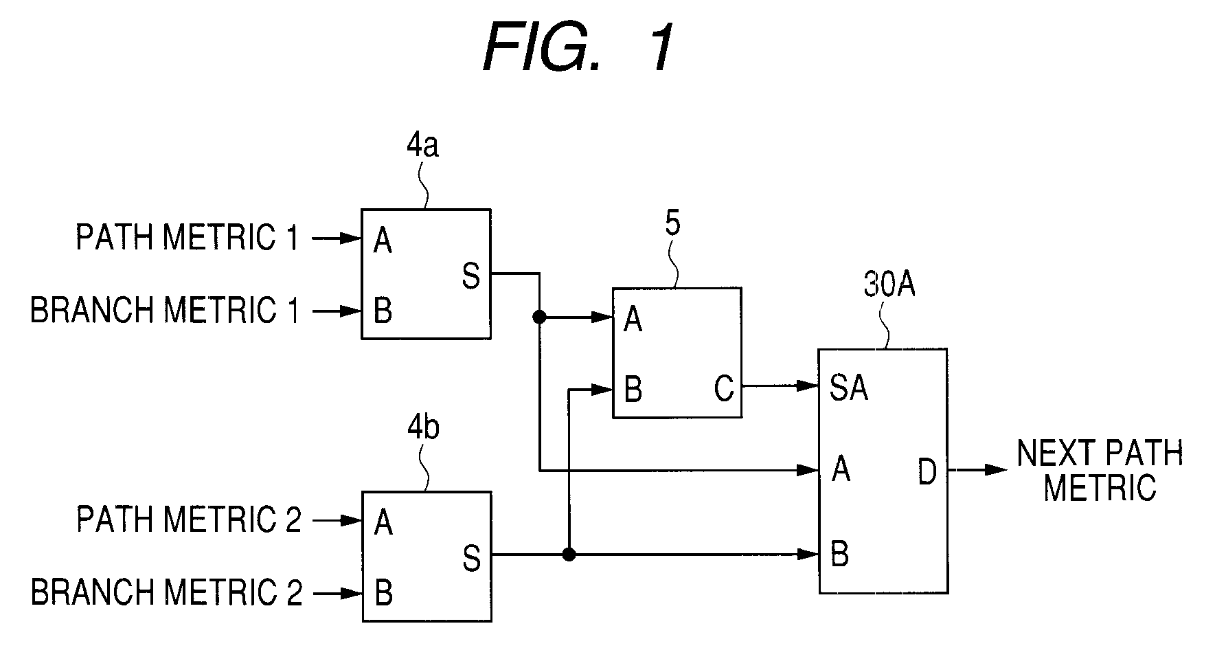
[0045]In the 3-input selection circuit 10, a control signal SM and a test signal SI supplied from a not-shown control circuit are given to a control input part SA and an input part A, respectively. Output signals D1 and D2 corresponding to addition results in not-shown two adders (corresponding to the adders 4a and 4b shown in FIG. 2) are supplied to input parts B and C, respectively. A selection signal SELL as a binary signal output from a not-shown comparator (cor...
second embodiment
B. Second Embodiment
[0051]A scan flip flop circuit of a second embodiment according to the present invention will now be described with reference to FIGS. 6 and 7.
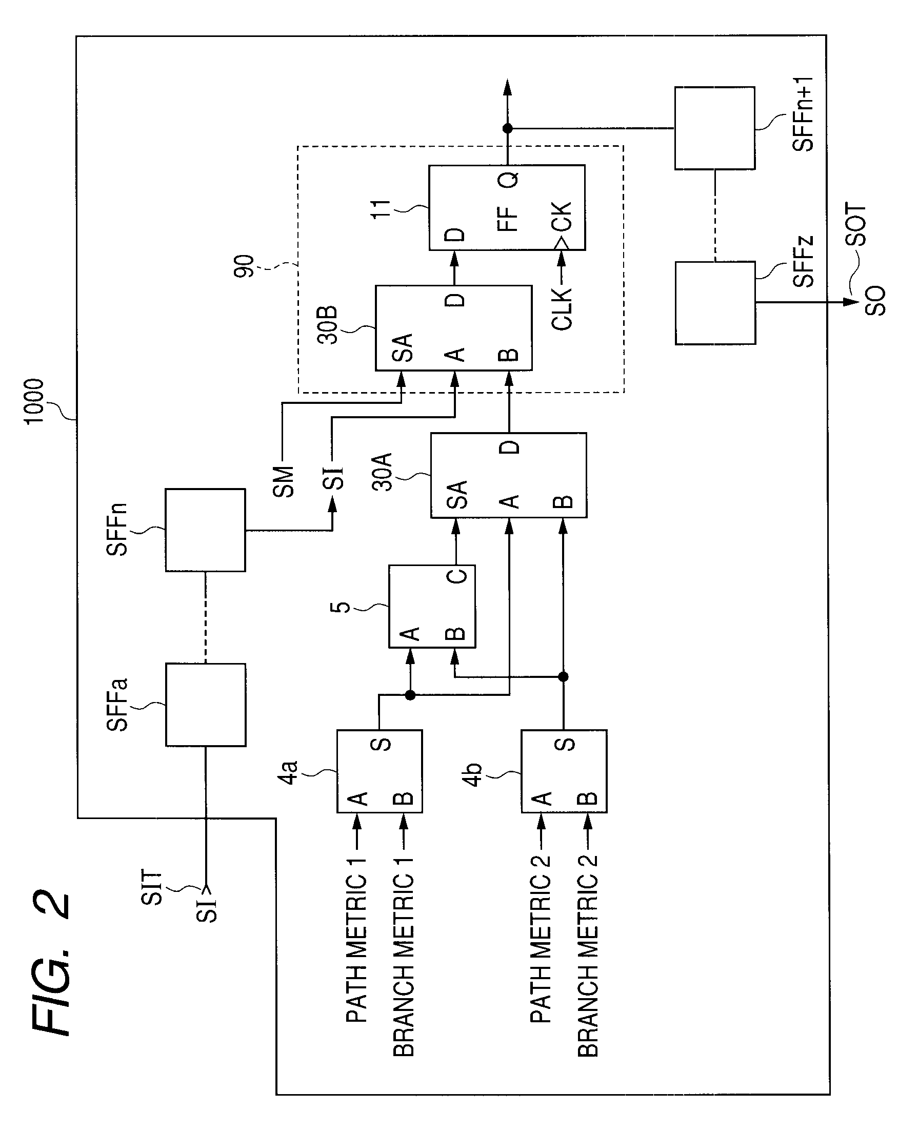
[0052]FIG. 6 is a block diagram showing the configuration of a scan flip flop circuit 200 with a selector. The scan flip flop circuit 200 has three 2-input selection circuits 30a, 30b, and 30c (first, second, and third 2-input selection circuits) in place of the 3-input selection circuit 10 shown in FIG. 3. The same reference numerals are designated to the same components as those of the scan flip flop circuit 100 with a selector shown in FIG. 3 and repetitive description will not be repeated.
[0053]Each of the selection circuits 30a to 30c is a circuit for outputting a signal supplied to an input part A to an output part D when the logical value of a signal supplied to a control input part SA is “1”, and outputting a signal supplied to an input part B to the output part D when the logical value of a signal supplied to the ...
third embodiment
C. Third Embodiment
[0064]A scan flip flop circuit of a third embodiment according to the present invention will now be described with reference to FIG. 8.
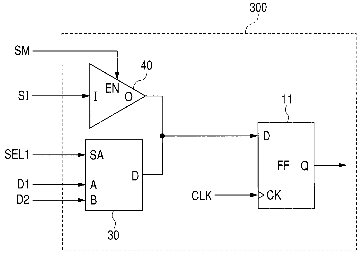
[0065]FIG. 8 is a block diagram showing the configuration of a scan flip flop circuit 300 with a selector. The scan flip flop circuit 300 has a tristate circuit 40 and a 2-input selection circuit 30 for selecting one signal from two input signals in place of the 3-input selection circuit 10 shown in FIG. 3.
[0066]In the tristate circuit 40, a test signal SI is output from an output part O in the case where the test signal SI and the control signal SM supplied from a not-shown control circuit are supplied to input parts I and EN, respectively, and the logical value of the control signal SM is “1”. When the logical value of the control signal SM is “0”, no signal is output. That is, the output part O is set to an open state or a high resistance (high impedance) state. Consequently, when the logical value of the control signal SM is “0...
PUM
 Abstract
Description
Claims
Application Information