Memory devices, stylus-shaped structures, electronic apparatuses, and methods for fabricating the same

a memory device and stylus-shaped technology, applied in the field of memory devices, can solve the problems of reducing the size of the heating electrode b>16, the ability to reduce the working current such as and the large amount of write current and reset current required to successfully change the phase state of the phase change material during cell operation

Inactive Publication Date: 2009-07-30
IND TECH RES INST
View PDF11 Cites 51 Cited by
  • Summary
  • Abstract
  • Description
  • Claims
  • Application Information

AI Technical Summary

Problems solved by technology

One problem found with conventional phase change memory cell structure as shown in FIG. 1, is that the amount of write current and reset current required to successfully change the phase state of the phase change material during cell operation is relatively large.
Reduction of the diameter D0 of the heating electrode 16, however, is limited by current photolithography process ability, thereby limiting size reduction of the heating electrode 16 and ability to decrease working currents such as write current and reset current.

Method used


Image

  • Memory devices, stylus-shaped structures, electronic apparatuses, and methods for fabricating the same
  • Memory devices, stylus-shaped structures, electronic apparatuses, and methods for fabricating the same
  • Memory devices, stylus-shaped structures, electronic apparatuses, and methods for fabricating the same

Examples


Embodiment Construction

[0040]The following description is of the best-contemplated mode of carrying out the invention. This description is made for the purpose of illustrating the general principles of the invention and should not be taken in a limiting sense. The scope of the invention is best determined by reference to the appended claims.

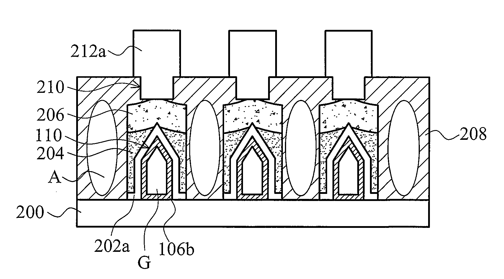
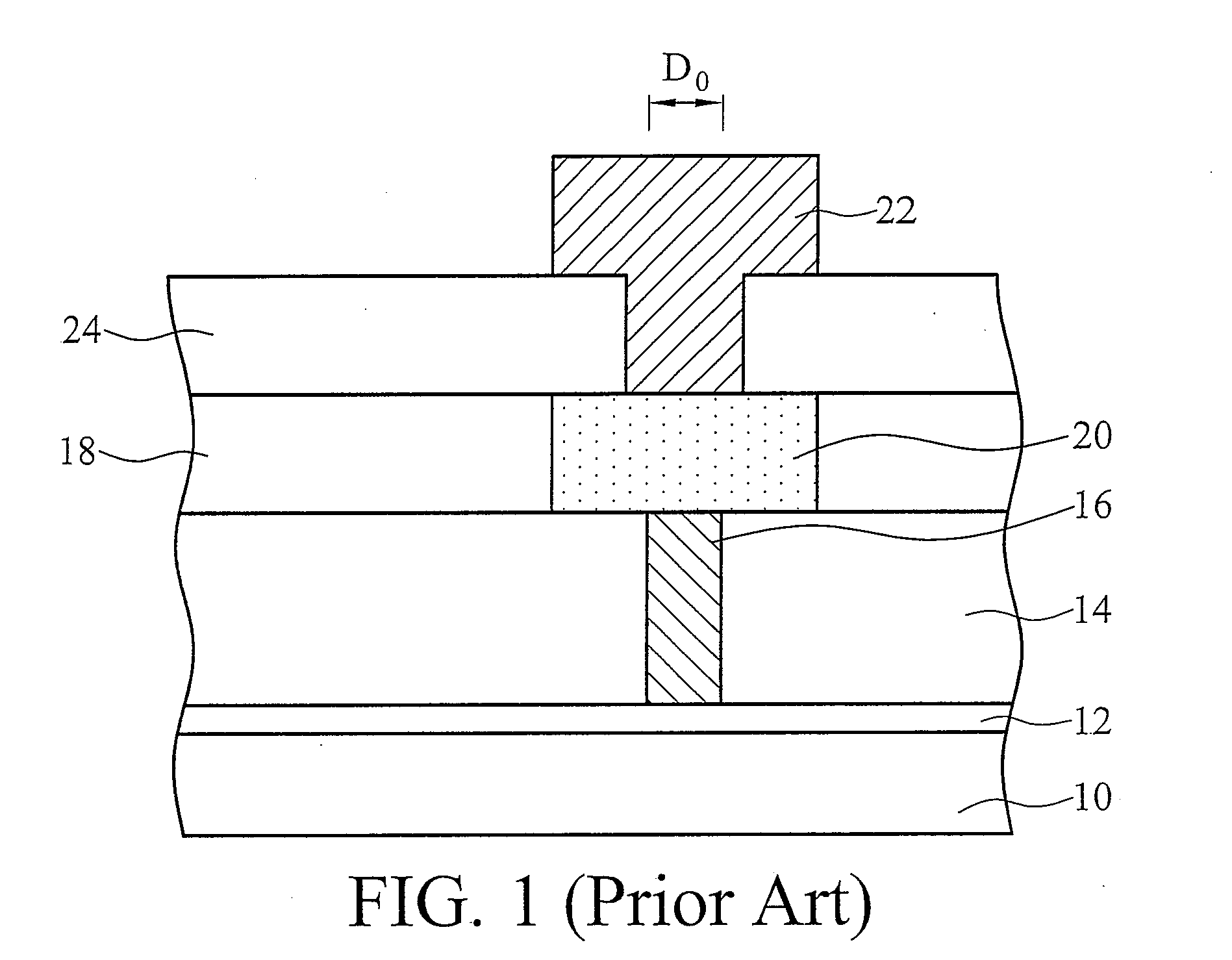
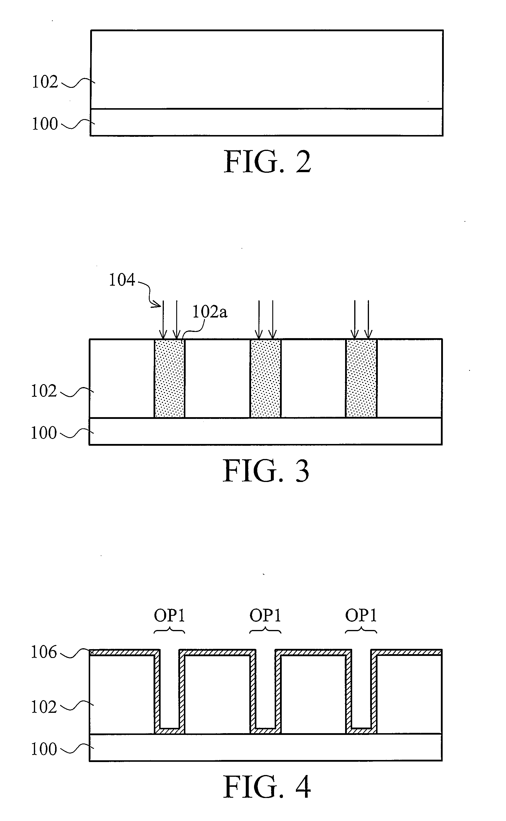
[0041]Embodiments of the invention are described as below incorporating FIGS. 2-27. FIGS. 2˜6 are schematic diagrams respectively showing fabrications in various fabrication steps of a stylus structure according to an embodiment of the invention. FIGS. 7˜11 are schematic diagrams respectively showing fabrications in various fabrication steps of a phase change memory device according to an embodiment of the invention. FIGS. 12˜18 are schematic diagrams memory devices, electronic apparatuses, fabrication systems, and phonic crystal structures according various embodiments of the invention that respectively use the hollow stylus-shaped structure illustrated in FIG. 6. FIG...


PUM

PropertyMeasurementUnit
thicknessaaaaaaaaaa
temperatureaaaaaaaaaa
thicknessaaaaaaaaaa

Abstract

An exemplary hollow stylus-shaped structure is disclosed, including a hollow column spacer formed over a base layer and a hollow cone spacer stacked over the hollow column spacer, wherein the hollow cone spacer, the hollow column spacer, and the base layer form a space, and sidewalls of the hollow cone spacer and the hollow column spacer are made of silicon-containing organic or inorganic materials.

Description

BACKGROUND OF THE INVENTION[0001]1. Field of the Invention[0002]The invention relates to memory devices, and more particularly to a phase change memory (PCM) device and a method for fabricating the same.[0003]2. Description of the Related Art[0004]Phase change memory devices are non-volatile, highly readable, and highly programmable, and require a relatively lower driving voltage / current. Current trends in phase change memory development are to increase cell density and reduce working currents such as write currents and reset currents thereof.[0005]Phase change material in a phase change memory device has at least two solid phases, a crystalline state and an amorphous state. Transformation between these two phases can be achieved by changing the temperature of the phase change material. The phase change material exhibits different electrical characteristics depending on its state. For example, in its amorphous state the material exhibits a higher resistivity than in the crystalline ...

Claims


Application Information

Patent Timeline
Patent Type & Authority Applications(United States)
IPC IPC(8): B29D22/00B32B1/08H01L45/00H01J1/62G21K5/00G02B6/10G11B5/187G03B27/54
CPCB82Y10/00Y10T428/13G02B6/1225G03B27/54G11B9/1409G11C13/0004H01L45/04H01L2924/0002B82Y20/00H01L45/1691H01L43/08H01L45/06H01L45/1233H01L45/124H01L45/126H01L45/1273H01L45/1293H01L45/144H01L45/146H01L45/1675H01L2924/00H10N70/8265H10N70/20H10N70/8413H10N70/8418H10N70/8616H10N50/10H10N70/231H10N70/068H10N70/8828H10N70/8833H10N70/063H10N70/826
Inventor CHEN, WEI-SU
Owner IND TECH RES INST
Why Eureka
Try Eureka