

Nanostructure based light emitting devices and associated methods
a light emitting device and nanostructure technology, applied in the direction of discharge tube luminescnet screens, discharge tube/lamp details, electric discharge lamps, etc., can solve the problems of reducing the commercial potential of quantum dots, affecting the light emitting effect, so as to achieve the effect of improving light emitting
- Summary
- Abstract
- Description
- Claims
- Application Information
AI Technical Summary
Benefits of technology
Problems solved by technology
Method used
Image

Examples
example
[0069] The following example illustrates an embodiment of the invention. It is to be understood that the following is only exemplary or illustrative of the application of the principles of the present invention. Numerous modifications and alternative compositions, methods, and systems may be devised by those skilled in the art without departing from the spirit and scope of the present invention. The appended claims are intended to cover such modifications and arrangements. Thus, while embodiments of the present invention has been described above with particularity, the following Example provides further detail in connection with what is presently deemed to be a practical embodiment of the invention.
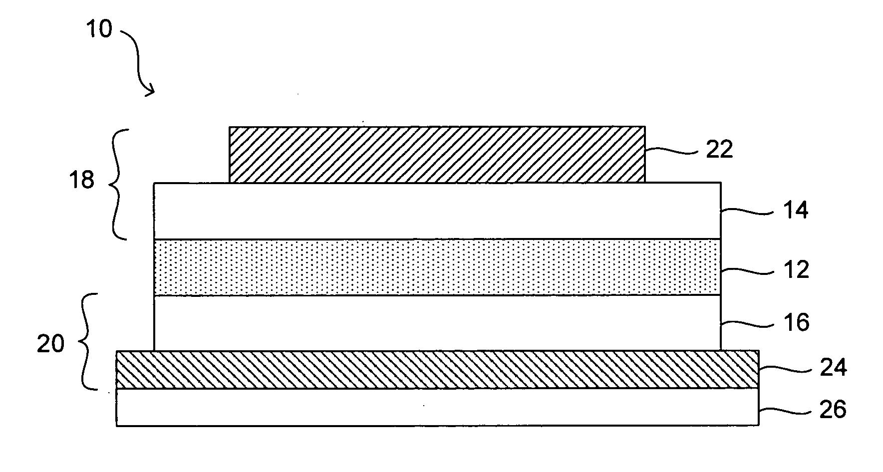
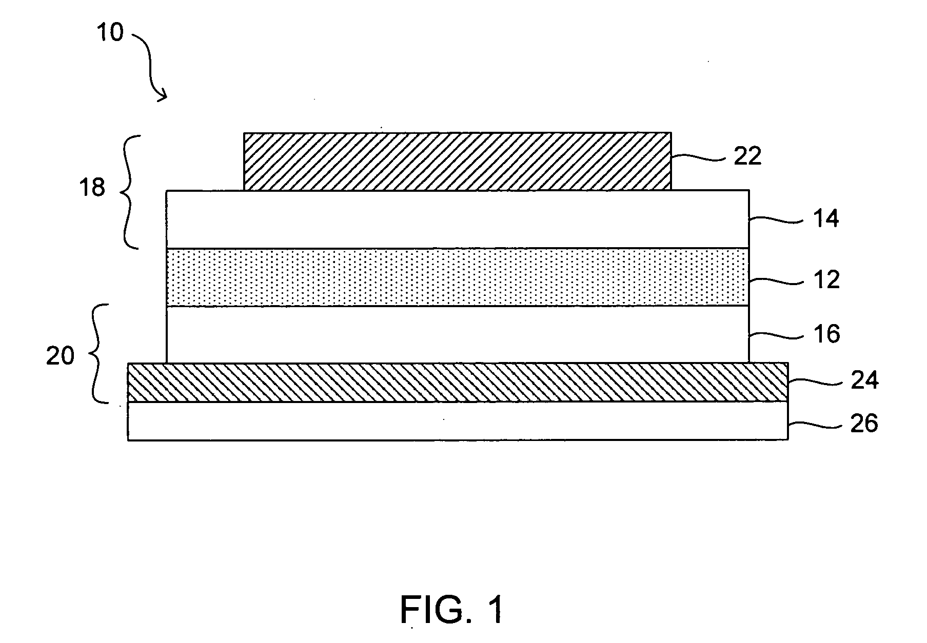
[0070] Fabrication of an LED having a luminescent wavelength between about 470 nm and 640 nm, depending on the nanostructure size, using CdSe—ZnS core-shell nanostructures is described. A high quality (optically transparent / smooth) glass substrate with a thin transparent indium tin oxide...
PUM
 Abstract
Description
Claims
Application Information