

Photovoltaic structure with a conductive nanowire array electrode
a photovoltaic structure and array electrode technology, applied in semiconductor devices, solid-state devices, nano-informatics, etc., can solve the problems of easy control, less efficiency of nanocrystalline structures, and high cost of single-crystal cells, so as to achieve the effect of easy control
- Summary
- Abstract
- Description
- Claims
- Application Information
AI Technical Summary
Benefits of technology
Problems solved by technology
Method used
Image

Examples
Embodiment Construction
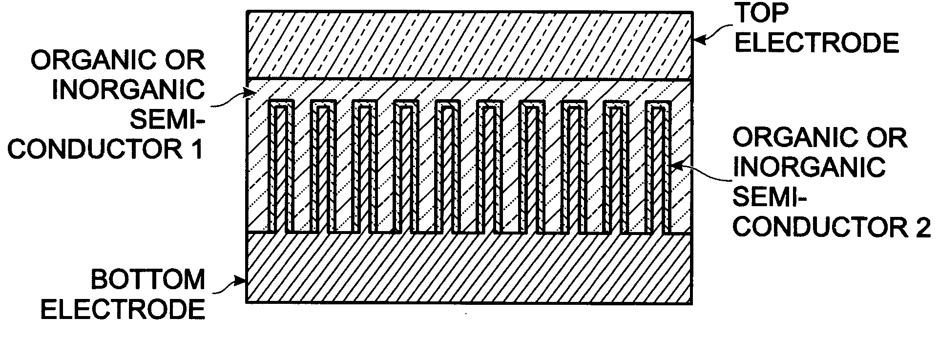
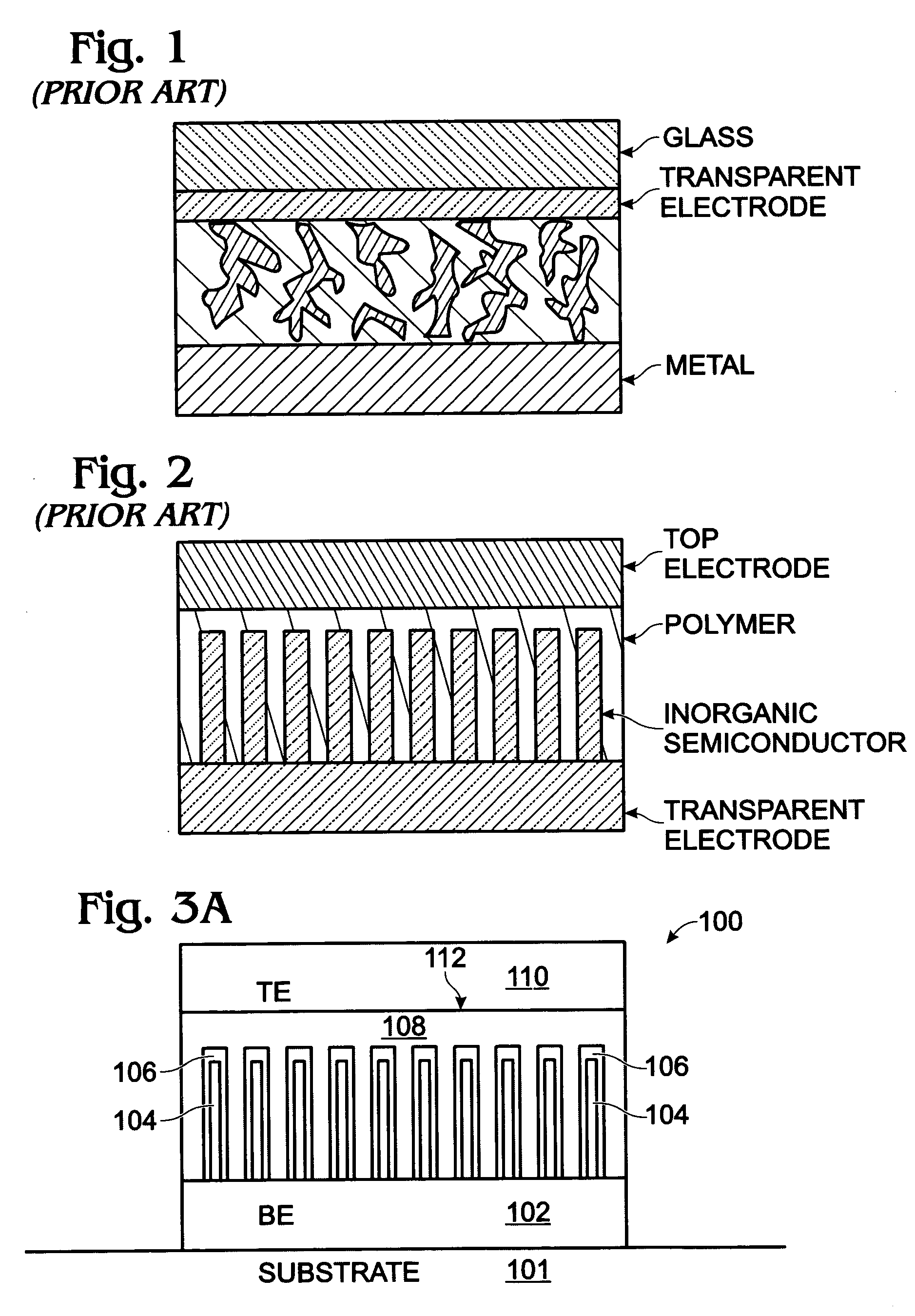
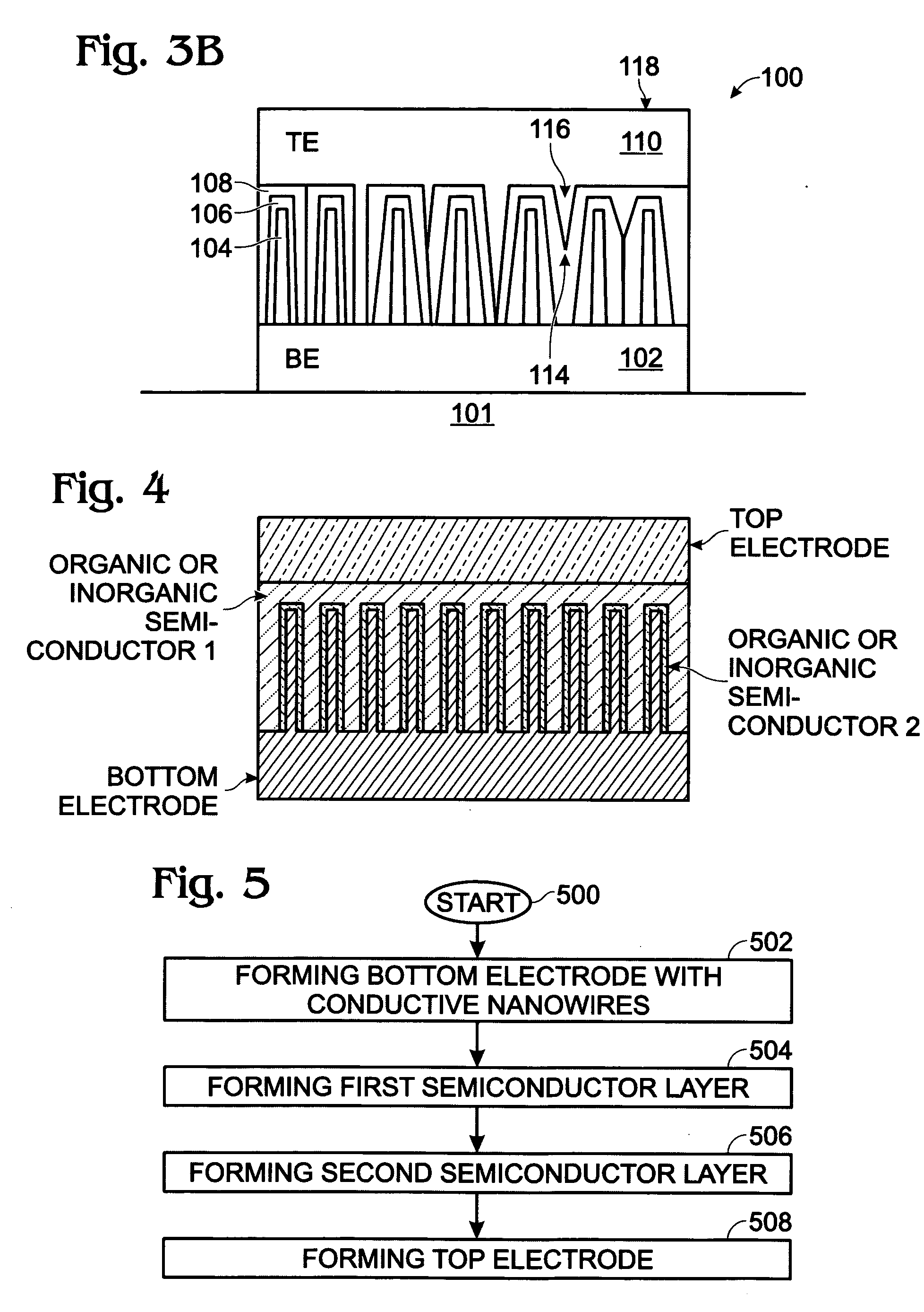
[0029]FIGS. 3A and 3B are partial cross-sectional views of a photovoltaic (PV) structure with a conductive nanowire array electrode. The PV structure 100 comprises a bottom electrode (BE) 102 with conductive nanowires 104. In some aspects, the bottom electrode is formed on a substrate such as a semiconductor material, glass, ceramic, metal, quartz, or plastic. The nanowires 104 are typically a material such as IrO2, In2O3, SnO2, carbon nanotube (CNT), or ITO. However, other conductive materials may also be used. The nanowire may alternately be called a nanorod, nanotube, or nanofiber. The nanowire is not limited to any particular diameter, length, or density. The nanowire may be single or multi-walled. A first semiconductor layer 106 of a first dopant type overlies the nanowires 104. A second semiconductor layer 108 of a second dopant type, opposite of the first dopant type, overlies the first semiconductor layer 106. A top electrode (TE) 110 overlies the second semiconductor layer ...
PUM
 Abstract
Description
Claims
Application Information