Wafer processing method

Active Publication Date: 2009-07-30
DISCO CORP
View PDF1 Cites 19 Cited by
  • Summary
  • Abstract
  • Description
  • Claims
  • Application Information

AI Technical Summary

Benefits of technology

[0019]According to the wafer processing method of the first aspect, since the blocking groove is already formed in the laminate along the street when the dividing groove is to be formed in the substrate of the wafer by the second laser beam application means in the above second trip blocking groove and dividing groove forming step and the first trip blocking groove and dividing groove forming step and a pulse laser beam having an output capable of forming the dividing groove in the substrate along the blocking groove, the laminate does not peel off and does not damage the devices. In addition, the above second trip blocking groove and dividing groove forming step and the first trip blocking groove and dividing groove forming step are carried out during one round trip of the chuck table to form the blocking groove and the dividing groove sequentially. Therefore, the method of the present invention is effective.
[0020]According to the wafer processing method of the second aspect, sin

Problems solved by technology

Since the above low-k film differs in the material from the substrate, it is difficult to cut it with the cutting blade together with the substrate.
That is, as the low-k film is extremely fragile like mica, when the above semiconductor wafer is cut alo

Method used


Image

  • Wafer processing method
  • Wafer processing method
  • Wafer processing method

Examples


Example

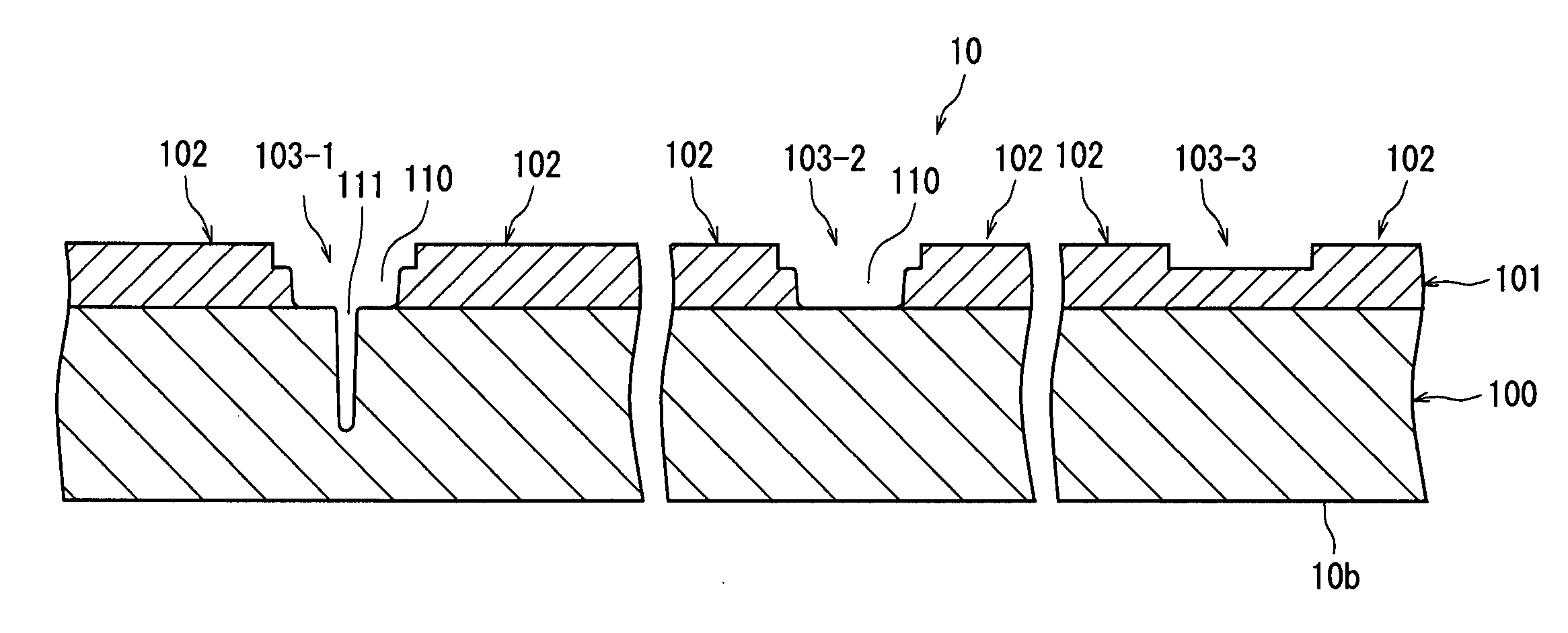
[0050]Preferred embodiments of the wafer processing method of the present invention will be described in detail hereinunder with reference to the accompanying drawings.

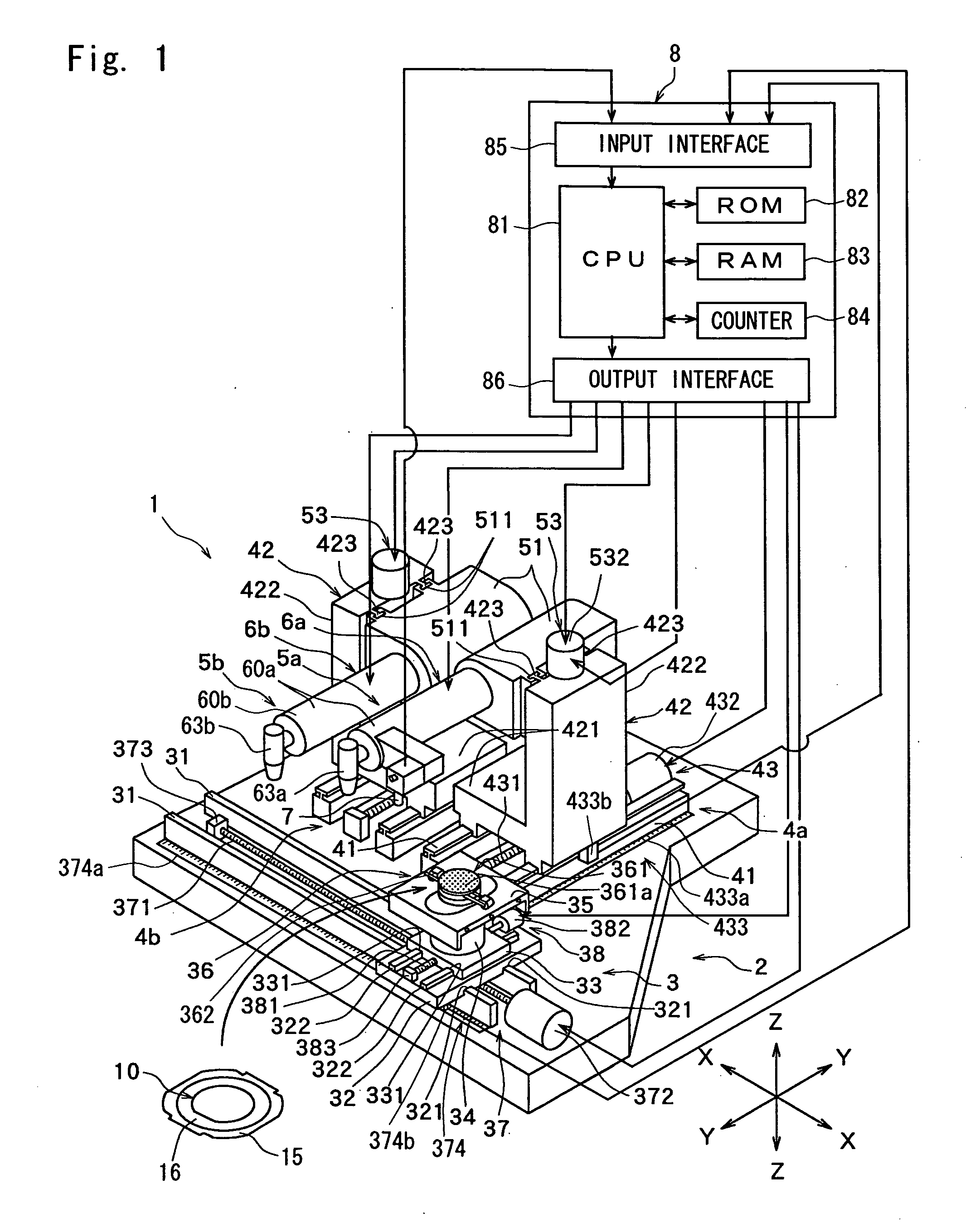
[0051]FIG. 1 is a perspective view of a laser beam processing machine for carrying out the wafer processing method of the present invention.

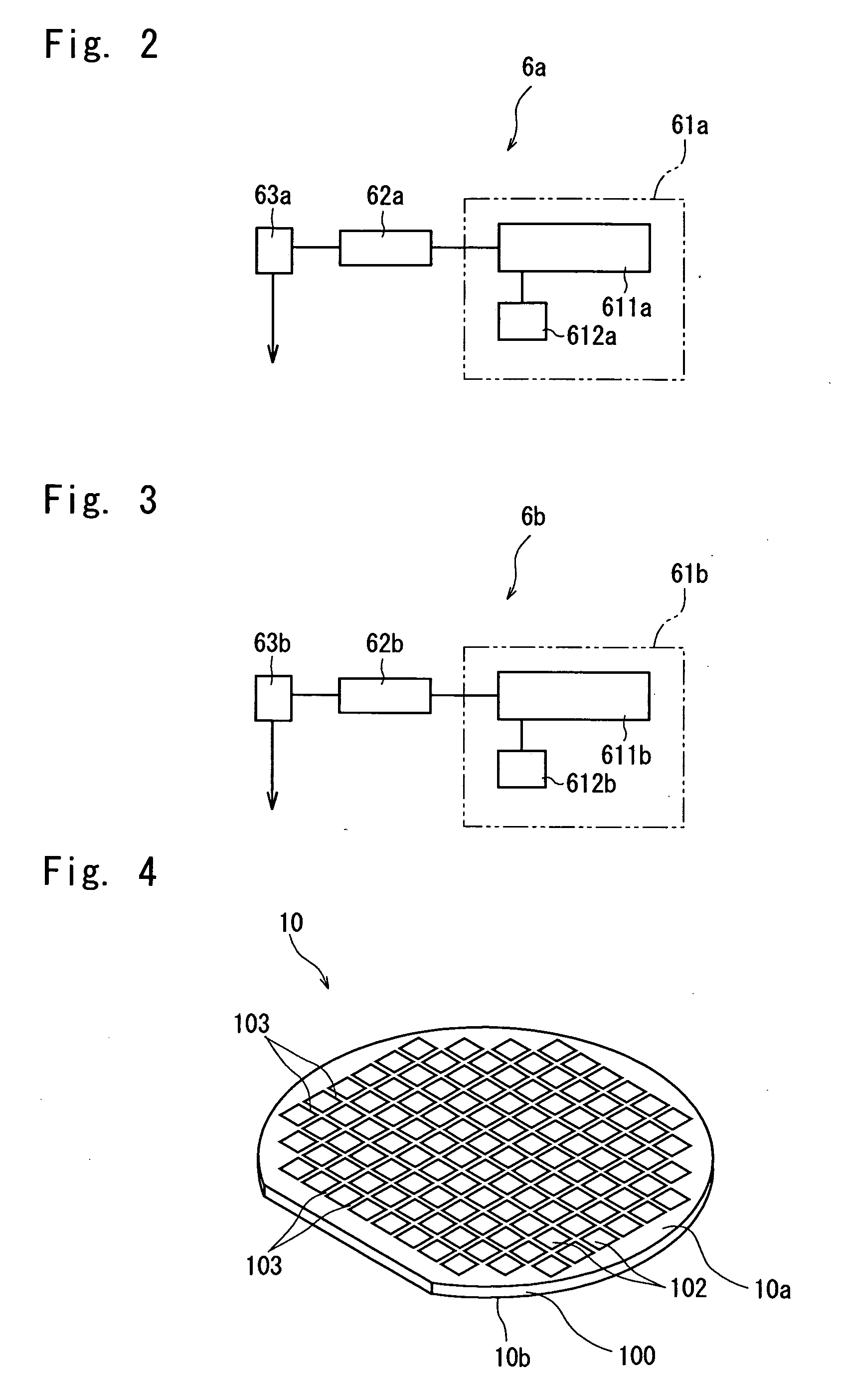
[0052]The laser beam processing machine 1 shown in FIG. 1 comprises a stationary base 2, a chuck table mechanism 3 for holding a workpiece, which is mounted on the stationary base 2 in such a manner that it can move in a processing-feed direction (X direction) indicated by an arrow X, a first laser beam application unit support mechanism 4a mounted on the stationary base 2 in such a manner that it can move in an indexing-feed direction (Y direction) indicated by an arrow Y perpendicular to the processing-feed direction (X direction) indicated by the arrow X, a first laser beam application unit 5a mounted on the first laser beam application-unit support mechanism 4a in such a manne...


PUM


Abstract

A method of processing a wafer having a plurality of devices which are composed of a laminate consisting of an insulating film and a functional film laminated on the front surface of a substrate, along streets for sectioning the plurality of devices, comprising a first trip blocking groove forming step for activating a first laser beam application means to form a blocking groove for dividing the laminate along a street of the wafer while moving the chuck table in a first direction in the processing-feed direction; a second trip blocking groove and dividing groove forming step for activating the first laser beam application means to form a blocking groove for dividing the laminate along a street next to the street which has undergone the first trip blocking groove forming step and also to form a dividing groove along the blocking groove formed by the first trip blocking groove forming step while moving the chuck table in a second direction in the processing-feed direction; and a first trip blocking groove and dividing groove forming step for activating the first laser beam application means to form a blocking groove for dividing the laminate along a street next to the street which has undergone the second trip blocking groove and dividing groove forming step and also, to form a dividing groove along the blocking groove formed by the second trip blocking groove and dividing groove forming step while moving the chuck table in a first direction in the processing-feed direction.

Description

FIELD OF THE INVENTION[0001]The present invention relates to a method of processing a wafer having a plurality of devices which are composed of a laminate consisting of an insulating film and a functional film on the front surface of a substrate, along streets for sectioning the plurality of devices.DESCRIPTION OF THE PRIOR ART [0002]As is known to people of ordinary skill in the art, a semiconductor wafer having a plurality of devices such as IC's or LSI's which are composed of a laminate consisting of an insulating film and a functional film and are formed in a matrix state on the front surface of a substrate such as a silicon substrate is formed in the production process of a semiconductor device. The above devices of the semiconductor wafer formed as described above are sectioned by dividing lines called “streets”, and the semiconductor wafer is divided along the streets to manufacture individual devices.[0003]Dividing along the streets of the above semiconductor wafer is genera...

Claims


Application Information

Patent Timeline
IPC IPC(8): H01L21/268B23K26/364B23K26/38
CPCB23K26/0648B23K26/0676B23K26/0807B23K26/0853H01L21/78B23K26/367B23K26/4075B23K26/409B23K2201/40B23K26/0884B23K26/082B23K26/364B23K26/40B23K2101/40B23K2103/172B23K2103/50
Inventor IIZUKA, KENTARO
Owner DISCO CORP
Why Eureka
Try Eureka