Plasma processing system
- Summary
- Abstract
- Description
- Claims
- Application Information
AI Technical Summary
Benefits of technology
Problems solved by technology
Method used
Image

Examples
Embodiment Construction
[0020]Hereinafter, the present invention will be described more fully with reference to the accompanying drawings, in which exemplary embodiments of the invention are shown. In the drawings, like reference numerals denote like elements.
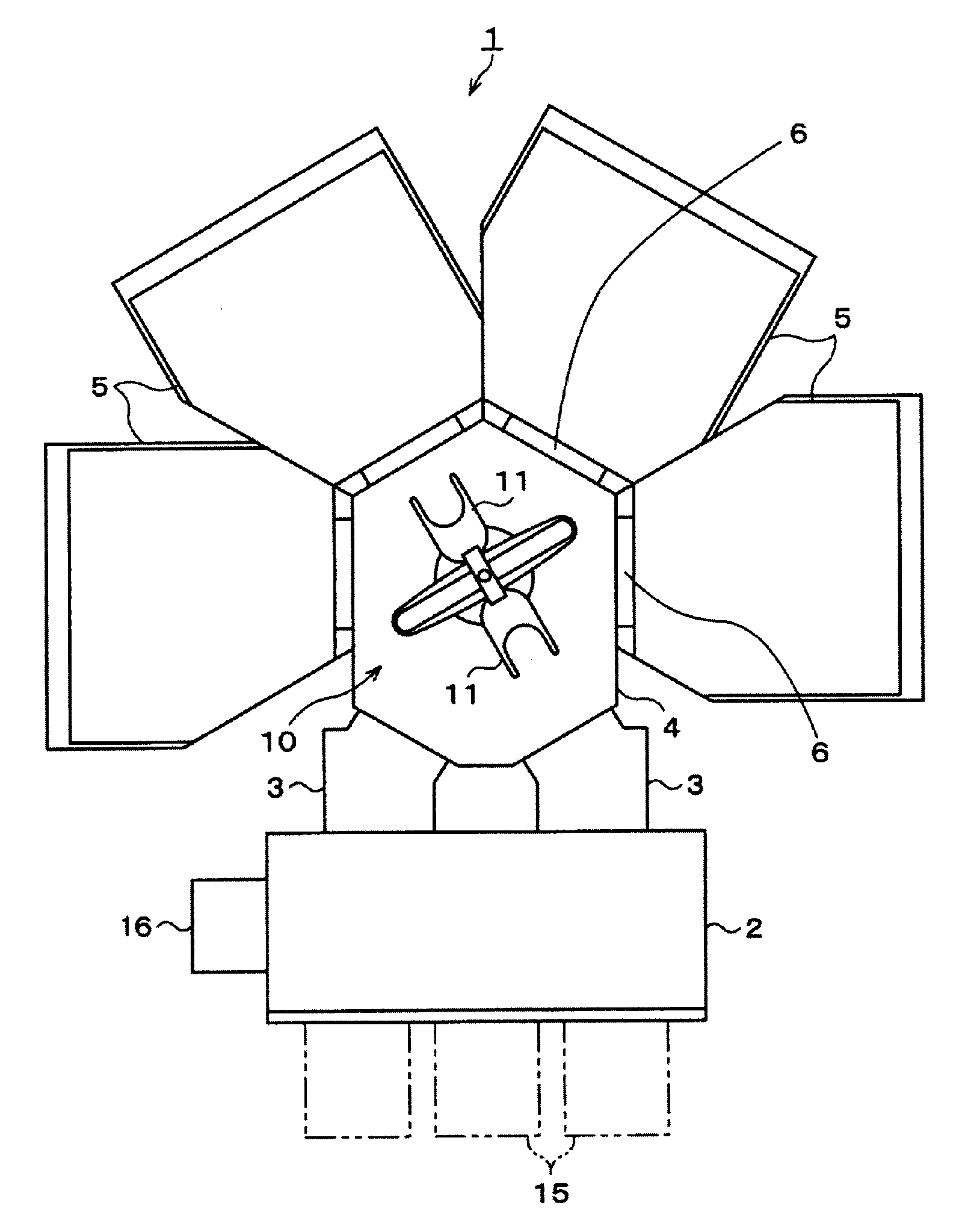
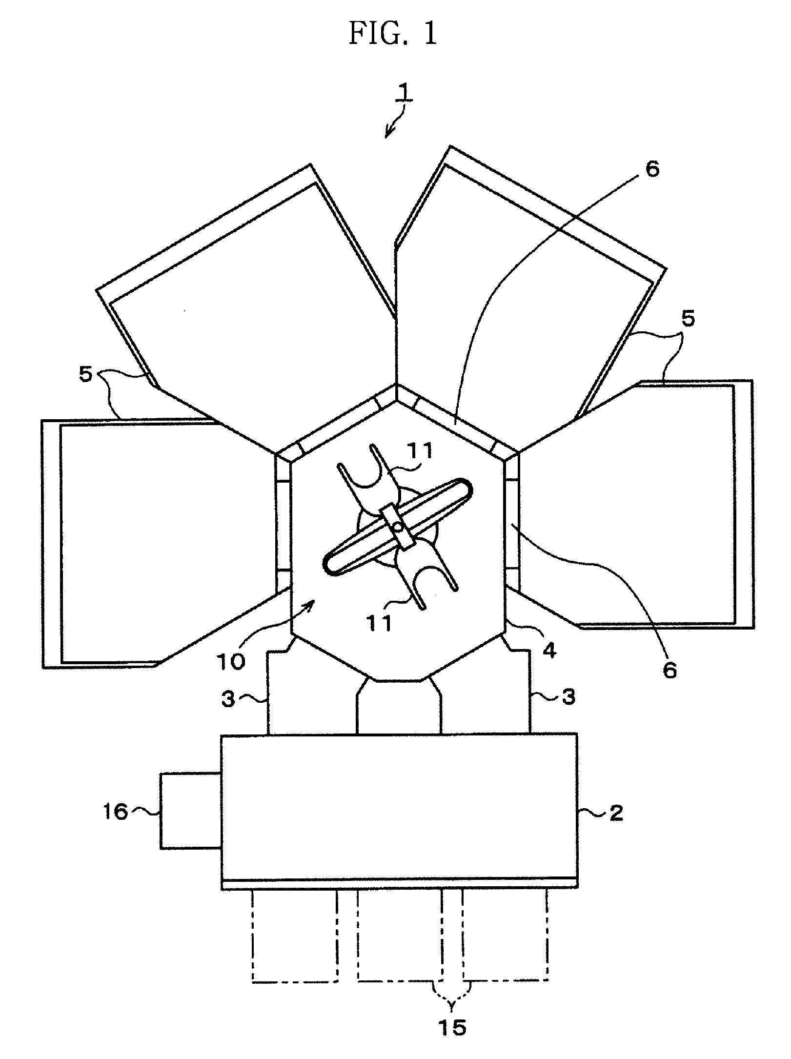
[0021]FIG. 1 is a diagram for describing a plasma processing system 1 according to an embodiment of the present invention. The plasma processing system 1 according to the current embodiment of the present invention includes a carry-in / out unit 2, which carries a wafer W as a substrate into and out of the plasma processing system 1, two load lock chambers 3, which are placed adjacent to the carry-in / out unit 2, a transfer chamber 4, which is placed adjacent to the each of the load lock chambers 3, and a plurality of plasma processing apparatuses 5, which are disposed around the transfer chamber 4. A gate valve 6 is mounted between each of the plasma processing apparatuses 5 and the transfer chamber 4.
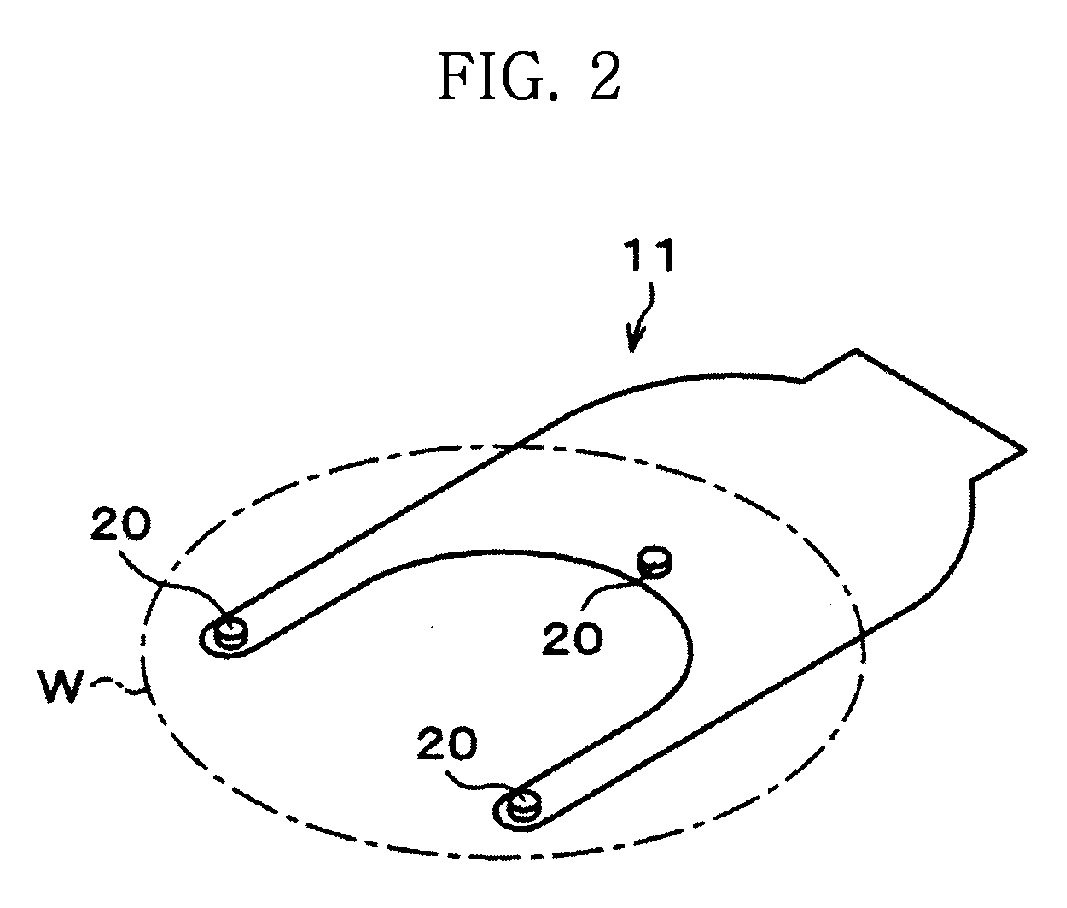
[0022]A transfer apparatus 10 is placed in the trans...
PUM
| Property | Measurement | Unit |
|---|---|---|
| Temperature | aaaaa | aaaaa |
Abstract
Description
Claims
Application Information
 - Generate Ideas
- Intellectual Property
- Life Sciences
- Materials
- Tech Scout
- Unparalleled Data Quality
- Higher Quality Content
- 60% Fewer Hallucinations
Browse by: Latest US Patents, China's latest patents, Technical Efficacy Thesaurus, Application Domain, Technology Topic, Popular Technical Reports.
© 2025 PatSnap. All rights reserved.Legal|Privacy policy|Modern Slavery Act Transparency Statement|Sitemap|About US| Contact US: help@patsnap.com