Chip card for insertion into a holder

a technology of chip card and holder, which is applied in the direction of sensing record carriers, instruments, and semiconductor/solid-state device details, etc., can solve the problems of high cost, limited volume available for chip production, and high production cost of conventional production methods, so as to achieve less complex chips, mass-produced more cheaply, and extended functional range

Inactive Publication Date: 2009-08-13
NXP BV
View PDF14 Cites 10 Cited by
  • Summary
  • Abstract
  • Description
  • Claims
  • Application Information

AI Technical Summary

Benefits of technology

[0021]It is further particularly advantageous if at least one further chip is arranged above a chip located on the second surface, the encapsulation enclosing all chips. By omitting the carrier material, a gain of approximately 200 μm in component height can be achieved, which is available for additional chips with a thickness of approximately 150 μm. A memory chip may, for instance, be placed piggyback-fashion on the processor chip of the chip card to extend its functional range. The integration of an additional processor chip covering the functions corresponding to the standard for “near field communication”, NFC in short, is also conceivable. Even the combination of digital and analog standard chips is made comparatively easy.
[0022]In the same way, it is advantageous if at least one further chip is added next to the chip located on the second surface, the encapsulation enclosing all chips. In this case, an additional chip is placed not above the existing chip but next to it. By omitting the flange required for bonding, volume for additional chips becomes available. The restrictions imposed by current technology on the available volume are expediently eliminated by the chip card according to the invention. It is, however, alternatively conceivable to use the acquired space for a cheaper, i.e. coarse, chip technology. Equivalent functionality can therefore be integrated into a larger and thus technically less complex chip.
[0023]In this context, it is expedient if at least one of the chips is designed as a processor and at least one other chip as a memory. A memory chip is, for instance, placed piggyback-fashion on top of the existing processor chip. This means that standard memory chips, which can be mass-produced more cheaply than a memory area on a processor chip, can be used. A further advantage of this variant of the invention lies in the fact that a processor chip of coarsely structured chip technology can be integrated with a memory chip of finely structured chip technology within one and the same chip card. This facility has not been available so far—owing to prior art production methods.
[0024]An advantageous variant of the invention features a chip card with at least one insertion direction and an encapsulation which facilitates insertion in the appropriate direction. The fact that the encapsulation is generally produced by injection molding opens up new possibilities with regard to the shaping of the chip card. The encapsulation may, for instance, be chamfered or radiused at the leading end in the direction of insertion to make the insertion of the chip card into the holder easier. This chamfer or radius can either be produced during the injection molding process or by milling or grinding. In view of to the punching process of the known production method, it has previously not been possible to produce a chip card of this shape.

Problems solved by technology

Quite apart from polluting the environment with unnecessary waste, the conventional production method is technically complex and therefore expensive because of the many process steps involved.
In addition, the volume available for the chip is extremely limited as a result of this technology.
The production of the chip either requires an expensive method allowing for small structures, or functionality has to be sacrificed.
In either case, conditions for producing chip cards are less than satisfactory.

Method used


Image

  • Chip card for insertion into a holder
  • Chip card for insertion into a holder
  • Chip card for insertion into a holder

Examples


Embodiment Construction

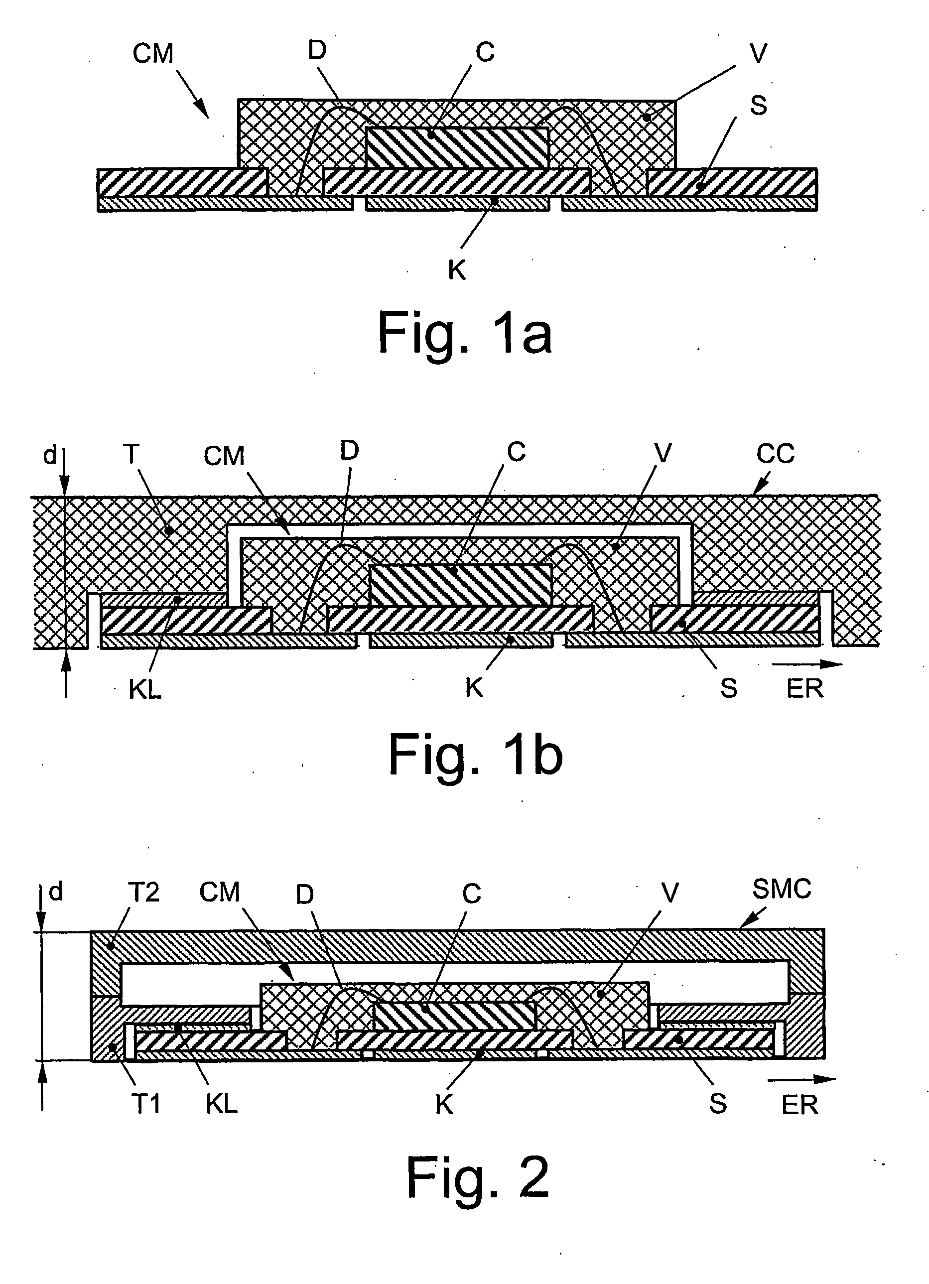
[0038]FIG. 1a shows a chip card module CM according to prior art. A contact field K is applied to a first side of the substrate S, while a chip C is bonded to the second side of the substrate S opposite the first side. The chip C is connected to the contact field K by wires D, said wires D running through holes in the substrate S which lead from the first to the second side of the substrate S. The chip C and the wires D are embedded in an encapsulation V protecting the chip C and the wires D from external influences while being significantly smaller than the substrate S in the present case.

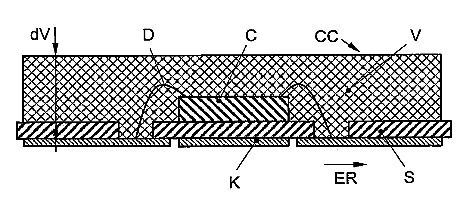
[0039]FIG. 1b shows a chip card CC, the chip card module from FIG. 1a having been bonded into a carrier material T. The carrier material T features a recess slightly larger than the chip card module CM, which has been produced by a method such as milling. The chip card module is installed into the carrier material T with the aid of an adhesive layer KL to form the chip card CC therewith. The carri...


PUM


Abstract

The invention relates to a chip card (CC), in particular a SIM card, inserted for operation into a holder (HH), which holder (HH) is equipped with electrical device contacts (GK) and a press-on device (AE). The chip card (CC) comprises a substrate (S), a contact field (K), a chip (C), and a single-piece encapsulation (V). According to the invention, the encapsulation (V) has a thickness (dV) which ensures that, on insertion of the chip card (CC), the encapsulation (V) has body contact with the press-on device (AE), the contact field (K) has body contact with the device contacts (GK), and the contact field (K) is reliably electrically contacted to the device contacts (GK). No further carrier material (T) is provided.

Description

FIELD OF THE INVENTION[0001]The invention relates to a chip card for insertion into a holder, which holder is equipped with electrical device contacts and a press-on device, comprising an electrically insulating planar substrate with a first surface and an opposing second surface, a metallic planar contact field applied to the first surface, a chip located on the second surface and electrically connected to the contact field, and a single-piece encapsulation located on the second surface and enclosing the chip.[0002]The invention further relates to an arrangement of several chip cards as described above.BACKGROUND OF THE INVENTION[0003]There are many applications for chip cards in the modem world, for instance as phone cards, ATM cards, access cards for Pay-TV and so-called “subscriber identity modules” or SIM cards for short. In order to produce the cards as cost-effectively as possible, a uniform size of 85×54 mm, i.e. the format of a credit card, was agreed. This ensures the easy...

Claims


Application Information

Patent Timeline
Patent Type & Authority Applications(United States)
IPC IPC(8): G06K7/00G06K19/06
CPCG06K19/07745H01L2924/01068H01L23/5388H01L24/45H01L2224/45144H01L2224/48228H01L2924/0105H01L2924/01079H01L2924/15184H01L2924/15311H01L23/49855H01L2924/01019H01L2224/48227H01L24/48H01L2924/00014H01L2924/181H01L2924/00012
Inventor SCHOBER, JOACHIM HEINZZENZ, CHRISTIAN
Owner NXP BV
Why Eureka
Try Eureka