Trench depth monitor for semiconductor manufacturing

a depth monitor and semiconductor technology, applied in the direction of instruments, microstructural devices, microstructured technology, etc., can solve the problems of reducing performance and reliability, and the depth cannot be measured only through destructive analysis techniques

Active Publication Date: 2009-08-13
ICEMOS TECH
View PDF47 Cites 256 Cited by
  • Summary
  • Abstract
  • Description
  • Claims
  • Application Information

AI Technical Summary

Benefits of technology

[0022]FIG. 5C is an enlarged top plan view of a process control module (PCM) from the wafer of FIG. 5A in accordance with a preferred embodiment of the present invention.

Problems solved by technology

In either of the examples of FIGS. 1B and 1C, sidewall doping will be affected, thereby resulting in decreased performance and reliability.
However, as the trenches 12 become narrower, at a width of 4 μm for example, the depth can only be measured via destructive analysis techniques, such as the use of a scanning electron microscope (SEM).

Method used


Image

  • Trench depth monitor for semiconductor manufacturing
  • Trench depth monitor for semiconductor manufacturing
  • Trench depth monitor for semiconductor manufacturing

Examples


Embodiment Construction

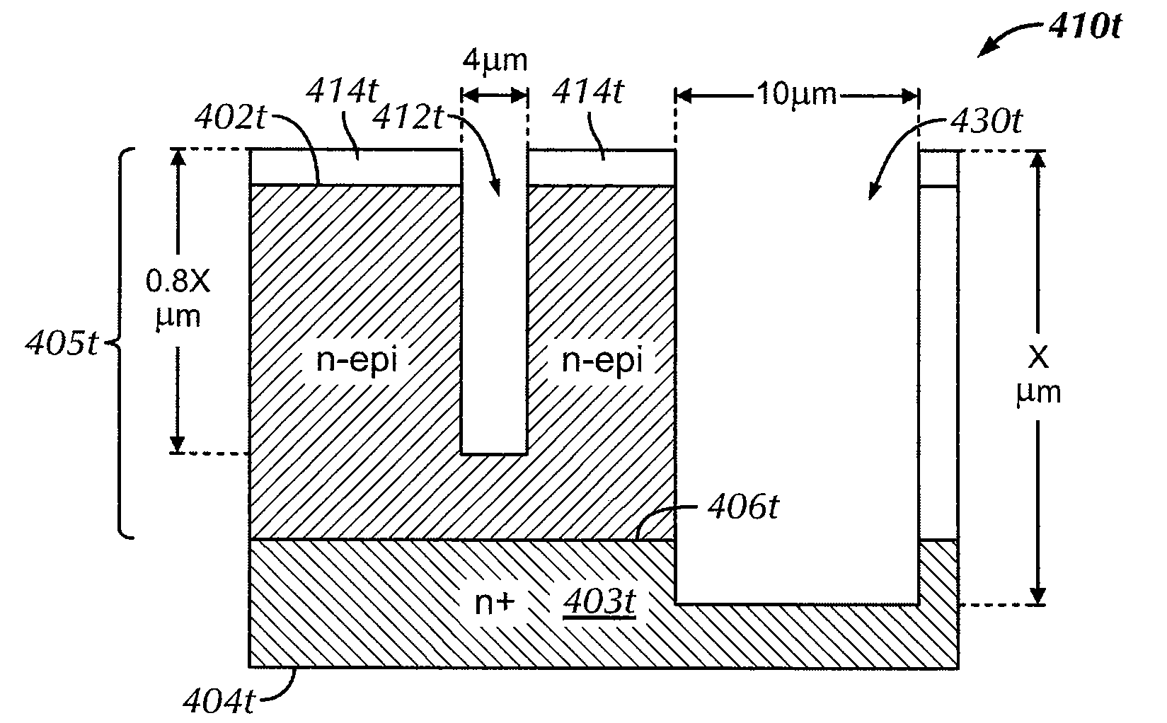
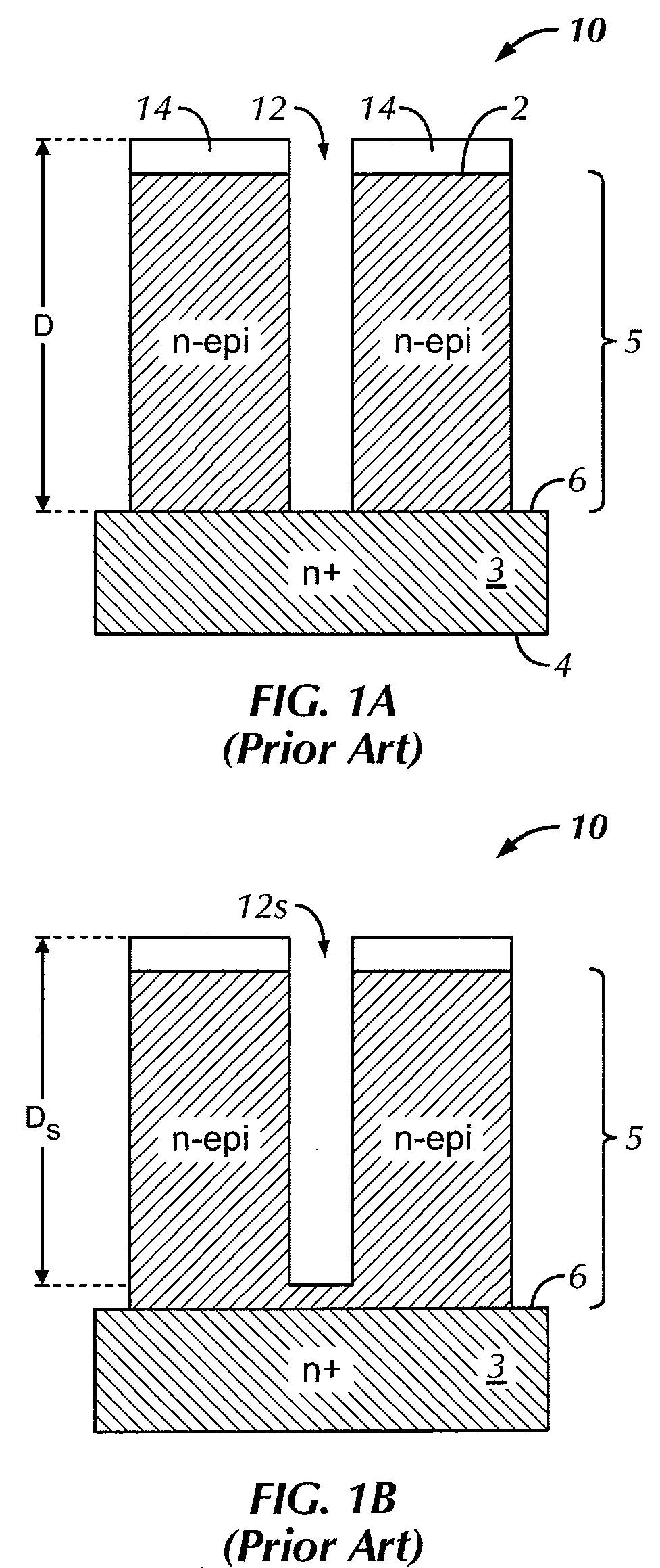
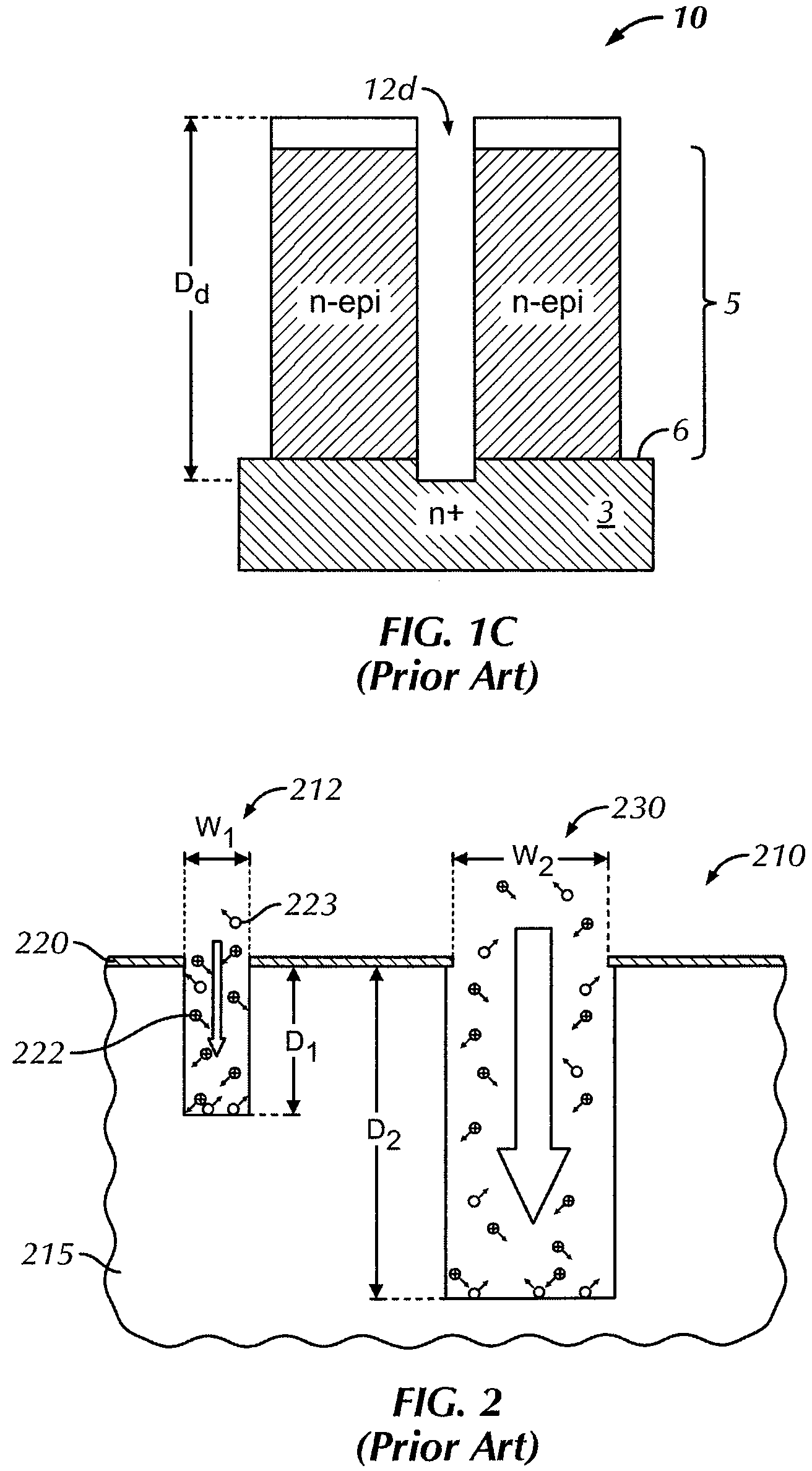
[0023]Certain terminology is used in the following description for convenience only and is not limiting. The words “right”, “left”, “lower”, and “upper” designate directions in the drawings to which reference is made. The words “inwardly” and “outwardly” refer to directions toward and away from, respectively, the geometric center of the device and designated parts thereof. The terminology includes the above-listed words, derivatives thereof, and words of similar import. Additionally, the words “a” and “an”, as used in the claims and in the corresponding portions of the specification, mean “at least one.”

[0024]As used herein, reference to conductivity will be limited to the embodiment described. However, those skilled in the art know that p-type conductivity can be switched with n-type conductivity and the device would still be functionally correct (i.e., a first or a second conductivity type). Therefore, where used herein, reference to n or p can also mean either n or p or p and n c...


PUM


Abstract

A method of manufacturing a semiconductor wafer having at least one device trench extending to a first depth position includes providing a semiconductor substrate having first and second main surfaces and a semiconductor material layer having first and second main surfaces disposed on the first main surface of the semiconductor substrate and determining an etch ratio. The least one device trench and at least one monitor trench are simultaneously formed in the first main surface of the semiconductor material layer. The at least one monitor trench is monitored to detect when it extends to a second depth position. A ratio of the first depth position to the second depth position is generally equal to the etch ratio.

Description

CROSS-REFERENCE TO RELATED APPLICATIONS[0001]This application claims the benefit of U.S. Provisional Patent Application No. 61 / 028,321, filed Feb. 13, 2008, entitled “Trench Depth Monitor for Semiconductor Manufacturing,” the entire contents of which are incorporated by reference herein.BACKGROUND OF THE INVENTION[0002]An embodiment of the present invention relates generally to a method of manufacturing a semiconductor device, and more particularly, to a method of manufacturing a semiconductor device by monitoring trench depth during processing.[0003]Since the invention of superjunction devices by Dr. Xingbi Chen, as disclosed in U.S. Pat. No. 5,216,275, the contents of which are incorporated by reference herein, there have been many attempts to expand and improve on the superjunction effect of his invention. U.S. Pat. Nos. 6,410,958, 6,300,171 and 6,307,246 are examples of such efforts and are incorporated by reference herein.[0004]Trench-type superjunction devices are expected to ...

Claims


Application Information

Patent Timeline
Patent Type & Authority Applications(United States)
IPC IPC(8): H01L21/02H01L23/00
CPCB81B2203/033B81C1/00619B81C99/0065B81C2201/0138H01L21/3065H01L22/12H01L2924/0002H01L22/26H01L29/0634H01L2924/13091H01L2924/00
Inventor GRIFFIN, HUGH J.ISHIGURO, TAKESHISUGIURA, KENJI
Owner ICEMOS TECH
Why Eureka
Try Eureka