
Semiconductor device and method for manufacturing the same

a technology of semiconductors and semiconductors, applied in the direction of variable capacitors, fixed capacitor details, fixed capacitors, etc., can solve the problems of increasing the aspect ratio of storage nodes, narrow space between storage nodes, and reducing the distance between electrodes, so as to prevent the leaning of storage nodes

Inactive Publication Date: 2009-08-20
SK HYNIX INC
View PDF6 Cites 21 Cited by
  • Summary
  • Abstract
  • Description
  • Claims
  • Application Information

AI Technical Summary

Benefits of technology

[0013]Embodiments of the present invention are directed to a semiconductor device and a method for manufacturing the same which prevents the leaning of storage nodes.

Problems solved by technology

In this regard, limitations exist in decreasing the distance between electrodes, that is, the thickness of the dielectric.
However, in the conventional art, as the size of cells decreases in order to accommodate the trend toward the high integration of semiconductor devices, not only does the aspect ratio of the storage nodes increases, but also the space between storage nodes becomes narrow.
However, when fixing the storage nodes in the form of a quadrangle, the support patterns are weak that causes the storage nodes to lean.
This separation causes defects in subsequent processes.
Further, when fixing the storage nodes in the form of a straight line, cracks are likely to occur between the support patterns and the storage nodes.
As a result, the breakdown voltage of the capacitors decrease, and capacitance often leak.

Method used


Image

  • Semiconductor device and method for manufacturing the same
  • Semiconductor device and method for manufacturing the same
  • Semiconductor device and method for manufacturing the same

Examples


Embodiment Construction

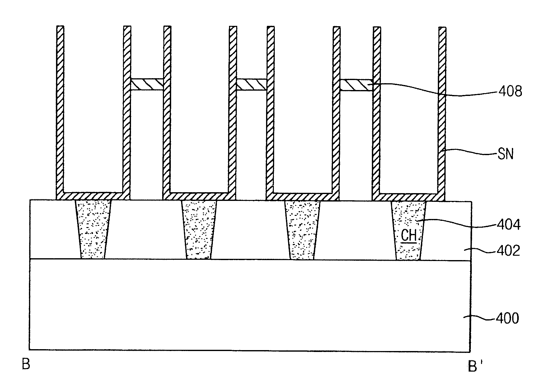
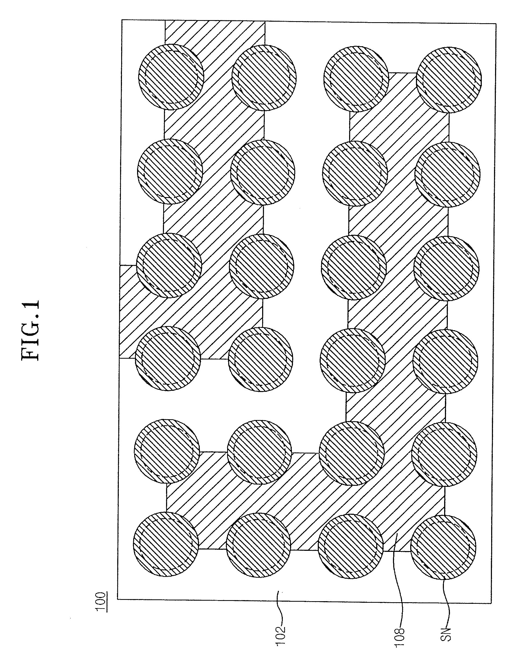
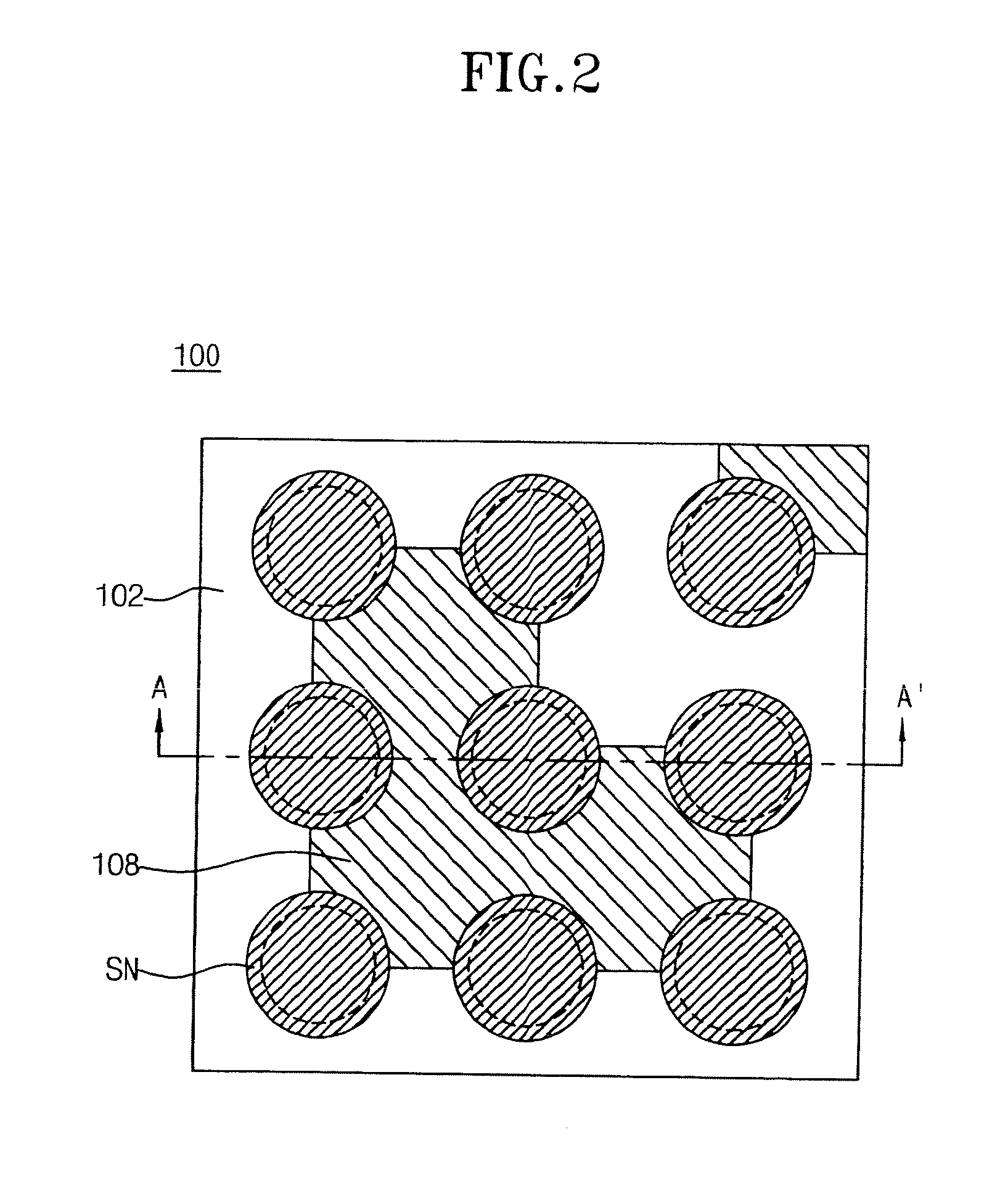
[0043]In the present invention, support patterns for fixing storage node are formed by manufacturing a semiconductor device having cylinder-shaped capacitors. The support patterns are formed to fix a plurality of storage nodes in the form of an ‘L’ or a ‘+’ when viewed from the top.

[0044]Accordingly, it is possible to prevent the storage nodes from leaning while conducting a wet dip-out process for removing an insulation layer. Thus, the capacitance of the capacitors is secured, and the manufacturing yield of a semiconductor device is increased.

[0045]Hereafter, the specific embodiments of the present invention will be described in detail with reference to the accompanying drawings.

[0046]FIG. 1 is a plan view illustrating a semiconductor device in accordance with one embodiment of the present invention.

[0047]Referring to FIG. 1, an interlayer dielectric 102 is formed on a semiconductor substrate 100, and storage node contact plugs (not shown) are formed in the interlayer dielectric 1...


PUM


Abstract

A semiconductor device that prevents the leaning of storage node when forming a capacitor having high capacitance includes a plurality of cylinder-shaped storage nodes formed over a semiconductor substrate; and support patterns formed to fix the storage nodes in the form of an ‘L’ or a ‘+’ when viewed from the top. This semiconductor device having support patterns in the form of an ‘L’ or a ‘+’ reduces stress on the storage nodes when subsequently forming a dielectric layer and plate nodes that prevents the capacitors from leaking.

Description

CROSS-REFERENCE TO RELATED APPLICATIONS[0001]The present application claims priority to Korean patent application number 10-2008-0015520 filed on Feb. 20, 2008, which is incorporated herein by reference in its entirety.BACKGROUND OF THE INVENTION[0002]The present invention relates generally to a semiconductor device and a method for manufacturing the same, and more particularly to a semiconductor device and a method for manufacturing the same for preventing the leaning of storage nodes.[0003]With increasing demand for semiconductor memory devices, various techniques for obtaining a capacitor having high capacitance have been proposed in the art. The capacitor has a structure in which a dielectric is interposed between storage nodes and plate nodes. As understood by ones skilled in the art, the capacitance of the capacitor is proportional to the surface area of an electrode and the dielectric constant of the dielectric and is inversely proportional to the distance between electrodes,...

Claims


Application Information

Patent Timeline
Patent Type & Authority Applications(United States)
IPC IPC(8): H01L29/00H01L21/00
CPCH01L28/91H01L27/10852H10B12/033H10B12/00
Inventor CHO, HO JINPARK, CHEOL HWANSEO, JAE WOOKKIM, JONG KUK
Owner SK HYNIX INC
Features
  • Generate Ideas
  • Intellectual Property
  • Life Sciences
  • Materials
  • Tech Scout
  • Unparalleled Data Quality
  • Higher Quality Content
  • 60% Fewer Hallucinations
Learn More