

Semiconductor device and a method of manufacturing the sae
a technology of semiconductor devices and semiconductor substrates, applied in semiconductor devices, semiconductor/solid-state device details, instruments, etc., can solve the problem of reducing the reliability of semiconductor devices by peeling, and achieve the effect of improving the reliability of semiconductor devices and reducing the density of redistribution interconnects formed within the plane of semiconductor substrates
- Summary
- Abstract
- Description
- Claims
- Application Information
AI Technical Summary
Benefits of technology
Problems solved by technology
Method used
Image

Examples
embodiment 1
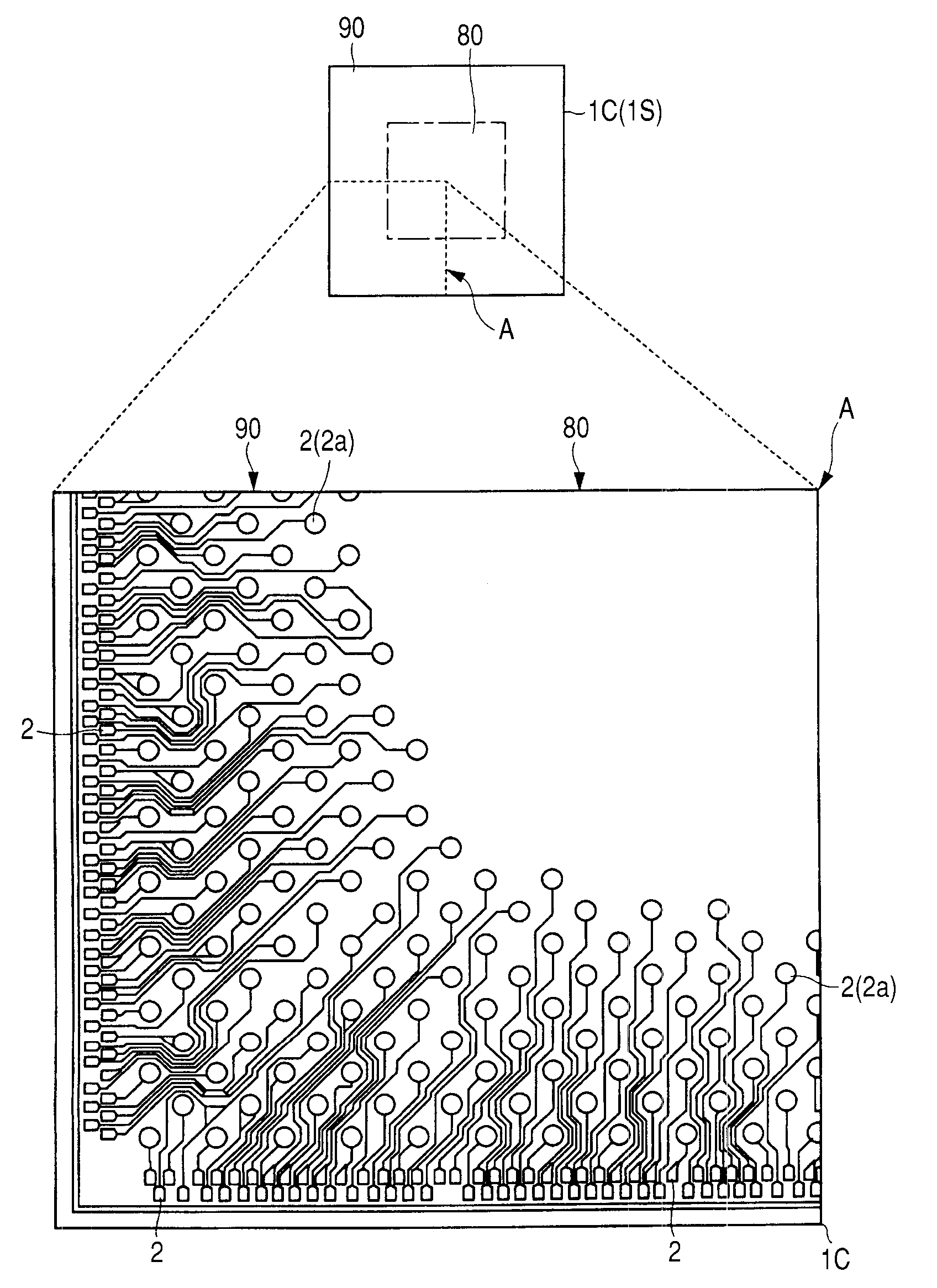
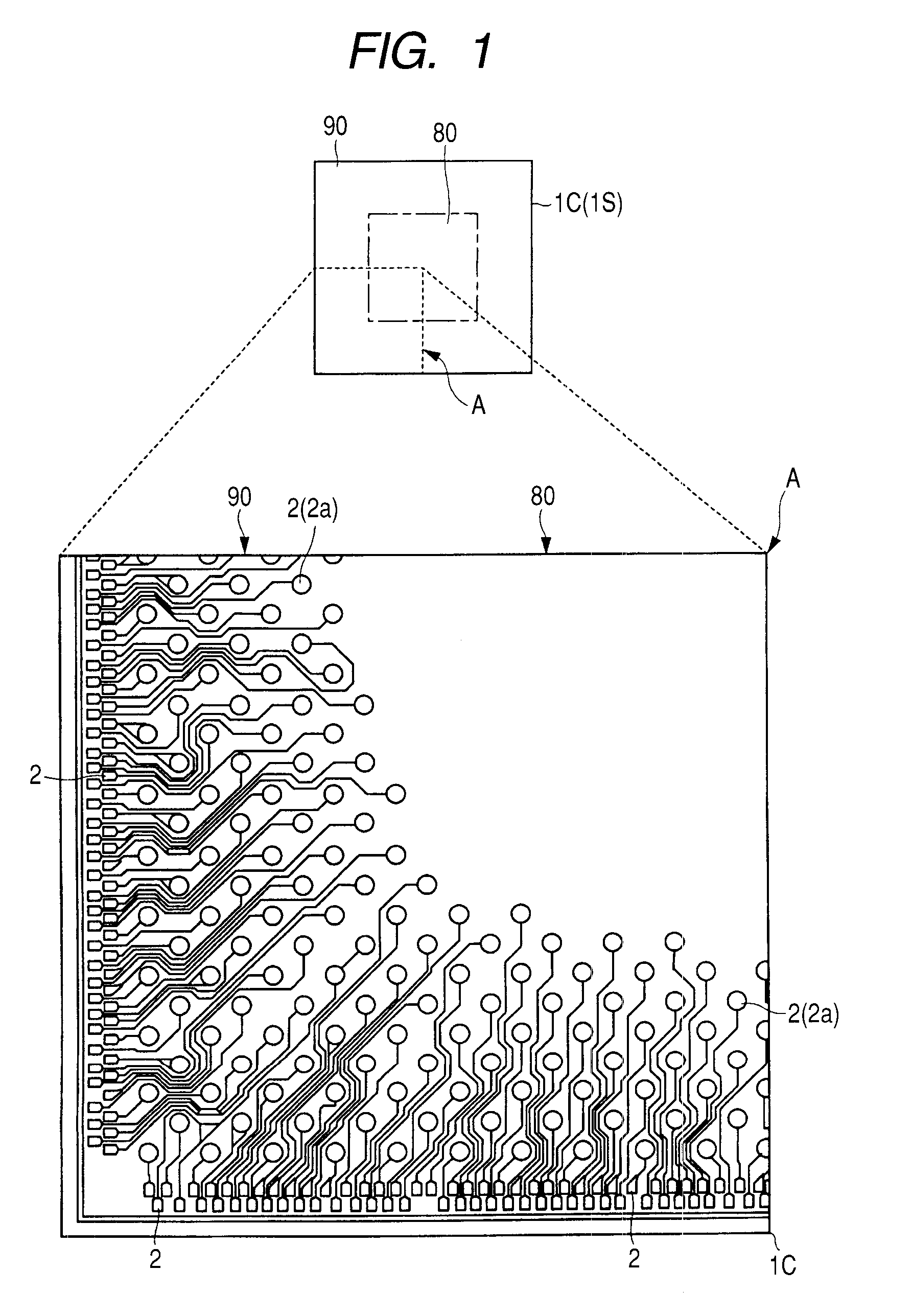
[0041](Embodiment 1) The semiconductor wafer of this embodiment is a semiconductor device having a CSP (Chip Size Package) structure and the WPP technology is used to manufacture the same. CSP is a generic term for packages which are the same or larger in size than a semiconductor chip. Since they can be reduced in size and weight and the length of an internal interconnect can be reduced, a signal delay and noise can be suppressed. The characteristic structure of the semiconductor device according to this embodiment will be described with reference to FIGS. 1 to 3.
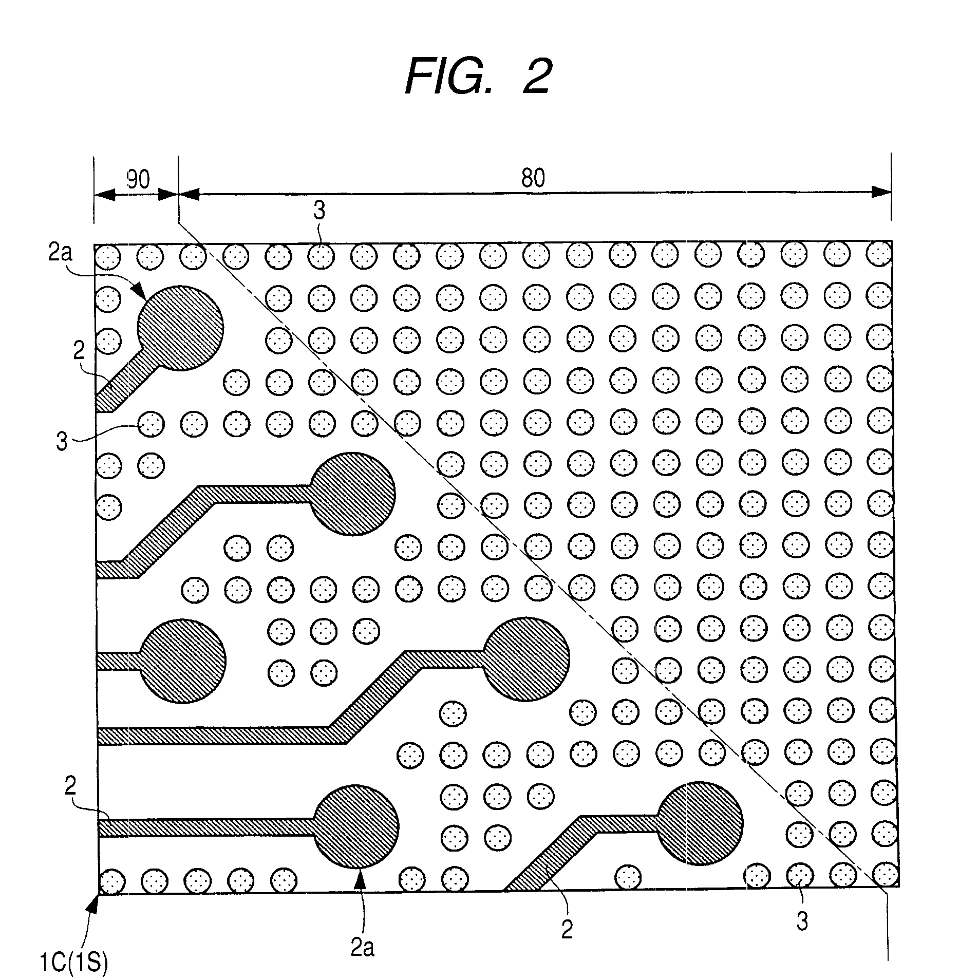
[0042]FIG. 1 is a plan view of a semiconductor chip 1C in this embodiment and an enlarged part (region A surrounded by the broken line) thereof. FIG. 2 is a more enlarged plan view of the semiconductor chip 1C shown in FIG. 1. Real patterns 2 and dummy patterns 3 shown in FIG. 2 are redistribution interconnects in the WPP technology. To make explanation easy, the dummy patterns 3 are not shown in FIG. 1. The real patterns ...
PUM
 Abstract
Description
Claims
Application Information