Liquid tank and ink jet printing apparatus
a liquid tank and ink jet printing technology, applied in the field of liquid tank and can solve the problems of difficult to increase the accuracy with which to determine the remaining amount of ink, disadvantages in cost, space, and ink housing efficiency, and achieve the effect of reducing the size of the ink jet printing apparatus and reducing the size of the liquid tank
- Summary
- Abstract
- Description
- Claims
- Application Information
AI Technical Summary
Benefits of technology
Problems solved by technology
Method used
Image
Examples
first embodiment
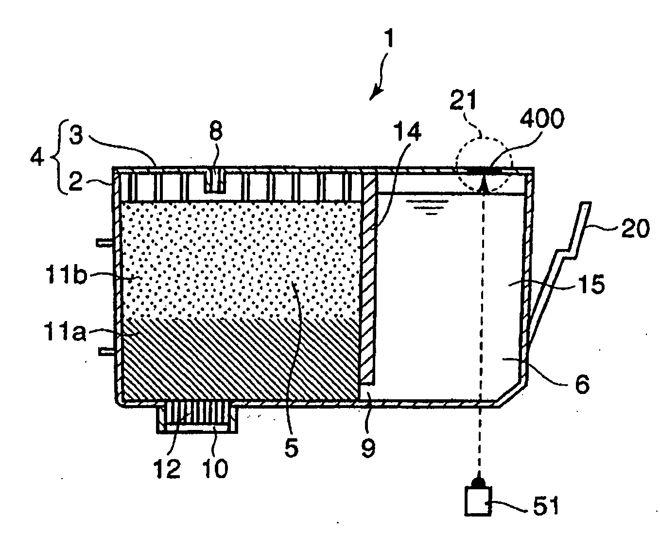
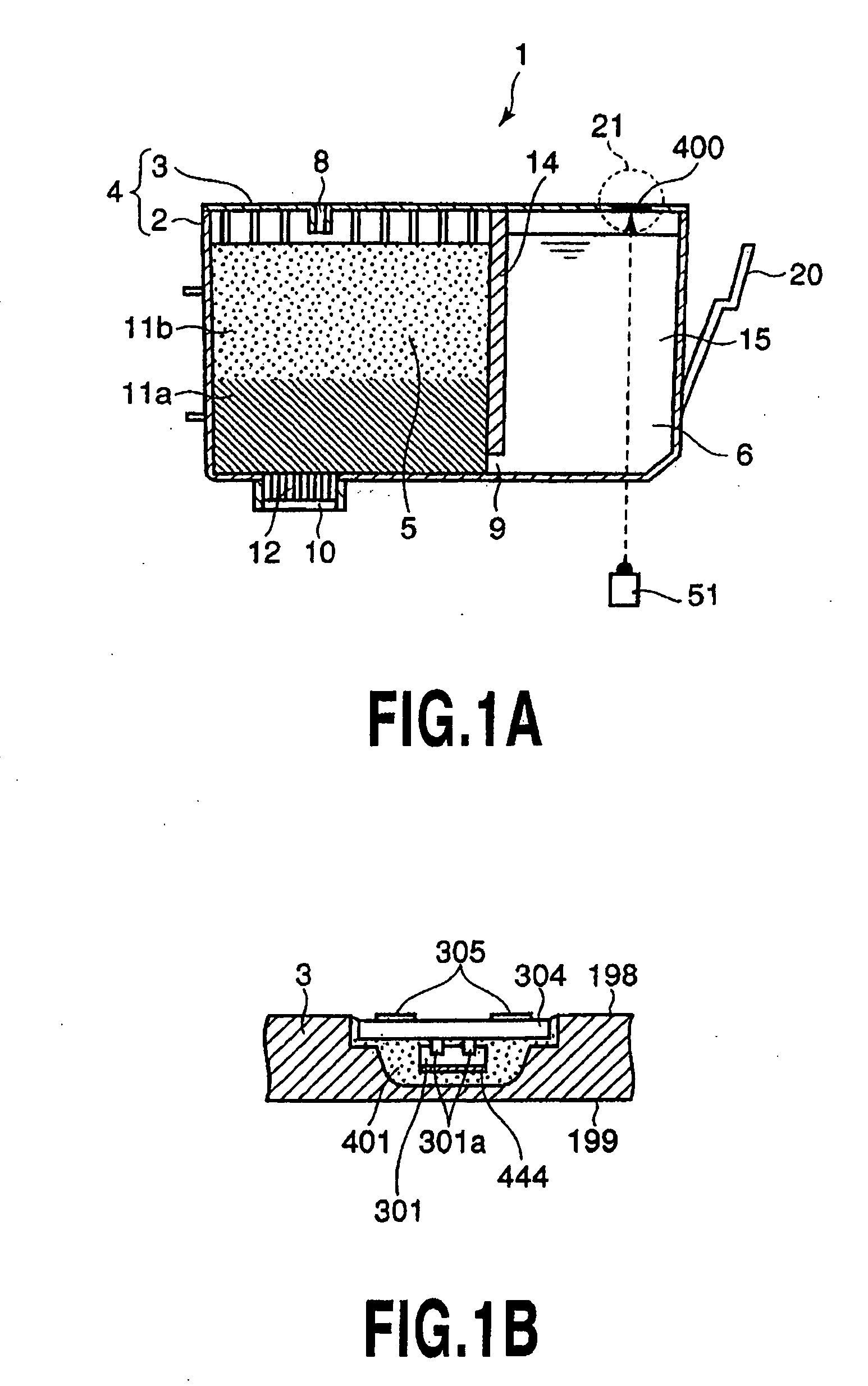
[0047]FIG. 1A is a sectional view schematically showing the configuration of an ink tank (liquid tank) 1 according to a first embodiment of the present invention.
[0048]In the ink tank 1, a housing 4 composed of a container 2 and a cover 3 is partitioned into two independent spaces using a partitioning wall 14; the spaces are in communication only via a communication portion 9 in the lower part of the partitioning wall 14. One of the two spaces is a negative pressure generating member housing chamber 5 in which two types of negative pressure generating members 11a and 11b are stacked and housed. The other space is an ink accommodating chamber (liquid accommodating chamber) 6.
[0049]The ink tank 1 is detachably installed on a carriage (not shown) in an ink jet printing apparatus main body using a lever 20; the carriage can be reciprocated. An ink supply port 10 is formed in a bottom wall of the negative pressure generating member accommodating chamber 5; an ink lead-out member 12 is pl...
second embodiment
[0078]FIG. 9A is a schematic diagram of an ink remaining amount sensing module provided in an ink tank according to a second embodiment of the present invention.
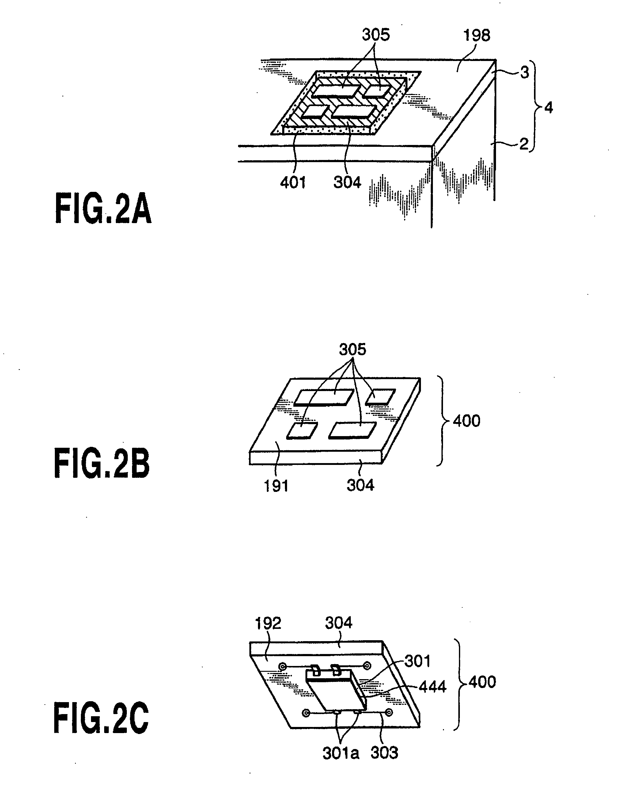
[0079]In the present embodiment, in contrast to the optical reflector 444 according to the first embodiment, an optical reflector 301c is formed utilizing a lead frame used to form a lead terminal 301a in mold-packaging the information storage element 301. Solder plating does not provide a high reflectance, so that the lead frame is desirably plated with gold. The optical reflector may be an aluminum reflection film, which exhibits a high reflectance of about 90% for light over a wide wavelength band. However, gold exhibits a reflectance of less than 40% in a near ultraviolet region but a high reflectance of 97 to 98% in an infrared region. Accordingly, gold can be effectively utilized as an optical reflector. Further, the gold reflector is desirable because it is more resistant to corrosion than the aluminum reflector.
third embodiment
[0080]FIG. 9B is a schematic diagram of an ink remaining amount sensing module provided in an ink tank according to a third embodiment of the present invention.
[0081]In the present embodiment, an optical reflector 303a is composed of a wiring member formed in a wide area of a wiring pattern formed on a printed circuit board as the support substrate 304. As in the case of the second embodiment, the wiring member is desirably plated with gold. However, a copper pattern used for common wiring members may be used provided that a sealing adhesive can be used to form a barrier against external environments. Further, measures are desirably taken for corrosion, migration, and the like. However, if it is undesirable to increase costs by employing gold plating, the copper pattern may be plated with nickel. In this case, a reflectance (about 70%) is obtained which is comparable to that of the stainless steel mirror shown in the first embodiment.
PUM
 Abstract
Description
Claims
Application Information


