Multi-level dynamic memory device

a dynamic memory and multi-level technology, applied in the direction of information storage, static storage, digital storage, etc., can solve the problem that the capacitance of the cell capacitor cannot be ignored

Active Publication Date: 2009-08-20
SAMSUNG ELECTRONICS CO LTD
View PDF10 Cites 6 Cited by
  • Summary
  • Abstract
  • Description
  • Claims
  • Application Information

AI Technical Summary

Problems solved by technology

However, in recent years, with the development of cell capacitor manufacturing technologies, the capacitance of the cell capacitor has increased to become about one third of the capacitance of the bit line, and thus, the capacitance of the cell capacitor cannot be ignored.

Method used


Image

  • Multi-level dynamic memory device
  • Multi-level dynamic memory device
  • Multi-level dynamic memory device

Examples


Embodiment Construction

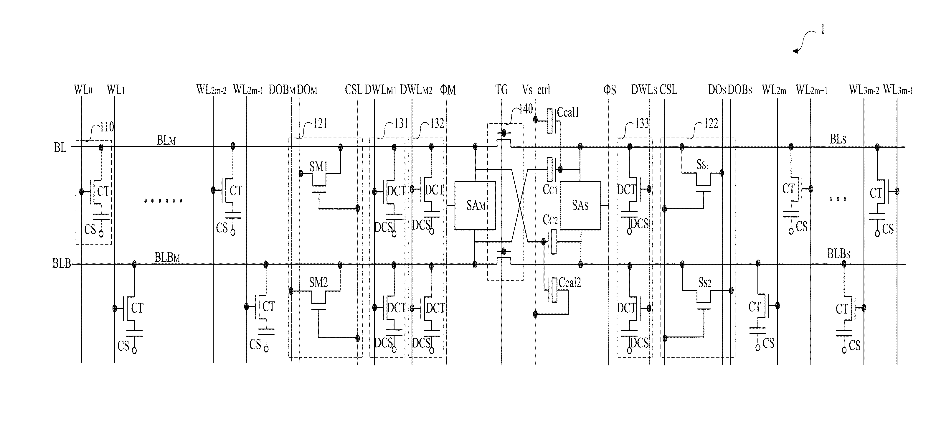
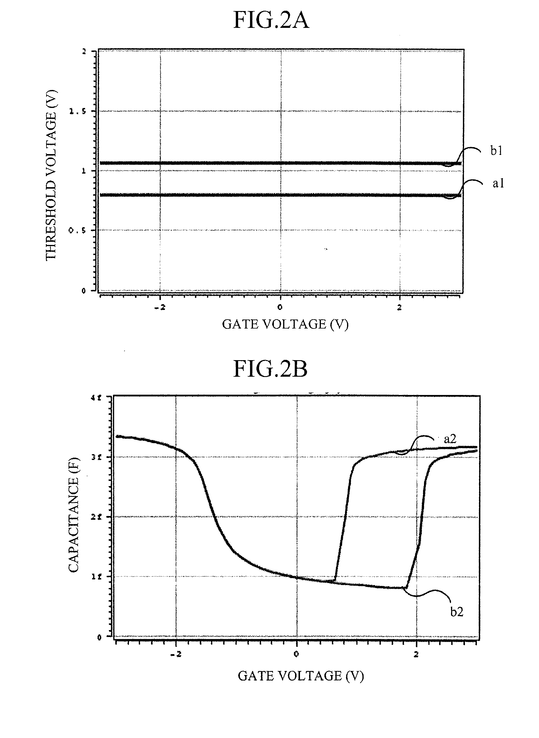
[0033]FIG. 1 is a circuit diagram illustrating a multi-level dynamic memory device according to an embodiment of the present invention, and FIGS. 2A and 2B are diagrams illustrating the reason why capacitances of first and second correction capacitors vary according to the variation of a first control voltage signal.

[0034]Referring to FIG. 1, in a multi-level dynamic memory device 1 according to the embodiment of the present invention, bits of each of memory cell 110 are provided to a bit line BL, then through first and second sense amplifiers SAM and SAS, and outputted through pairs of data lines DOM and DOBM, and DOS and DOBS.

[0035]A pair of bit lines BL and BLB is divided into a pair of main bit lines BLM and BLBM and a pair of sub-bit lines BLS and BLBS on the basis of a transfer transistor 140 that is controlled by a transfer signal TG. Capacitance at the pair of main bit lines BLM and BLBM may be twice as much as capacitance at the pair of sub-bit lines BLS and BLBS. In order ...


PUM


Abstract

A multi-level dynamic memory device includes a bit line pair that is divided into a main bit line pair and a sub-bit line pair, first and second sense amplifiers that are connected between the main bit line pair and between the sub-bit line pair, first and second coupling capacitors that are cross-coupled between the main bit pair and the sub-bit pair, respectively; and first and second correction capacitors that are connected in parallel to the first and second coupling capacitors, respectively, and whose capacitance is adjusted by a control voltage signal.

Description

CROSS REFERENCE TO RELATED APPLICATION[0001]This application is a divisional application of U.S. patent application Ser. No. 11 / 638,002, filed on Dec. 13, 2006, which claims the benefit of Korean patent application number 10-2005-0124005, filed on Dec. 15, 2005, in the Korean Intellectual Property Office, the contents of which applications are incorporated herein in their entirety by reference.BACKGROUND OF THE INVENTION[0002]1. Technical Field[0003]The present invention relates to a multi-level dynamic memory device, and more particularly, to a multi-level dynamic memory having an increased sensing margin.[0004]2. Description of the Related Art[0005]In recent years, various methods of storing more information in a limited wafer area have been developed. For example, sophisticated lithography methods and sophisticated lithography devices have been developed and used to manufacture more memory cells in a limited wafer area. In another method, one or more bits are stored in one memory...

Claims


Application Information

Patent Timeline
Patent Type & Authority Applications(United States)
IPC IPC(8): G11C11/24G11C7/00
CPCG11C7/06G11C7/14G11C7/18G11C2207/002G11C11/4097G11C11/4099G11C11/565G11C11/4091G11C8/14G11C11/4074
Inventor SONG, KI-WHAN
Owner SAMSUNG ELECTRONICS CO LTD
Why Eureka
Try Eureka