Storage system and data write method

a storage system and data technology, applied in the field of storage system and data write method, can solve the problems of waste of rewritable life (approximately 100,000 times per memory block), waste of low-performance data arrangement, waste of rewritable life of low-performance devices, etc., and achieve the effect of enhancing write performance and reducing the average write processing tim

Inactive Publication Date: 2009-08-20
HITACHI LTD
View PDF7 Cites 38 Cited by
  • Summary
  • Abstract
  • Description
  • Claims
  • Application Information

AI Technical Summary

Benefits of technology

[0007]The present invention was devised in view of the circumstances described above. This invention aims to suggest: a storage system that has high-performance device cache small-sized write data several times, and then writes it to a low-performance device, thereby reducing the average write processing time and enhancing write performance; and a data write method for such a storage system.

Problems solved by technology

Therefore, as a problem that might occur in the storage system, there is a possibility that the rewritable life (approximately 100,000 times per memory block) of flash memory in the low-performance device may be wasted.
This means that a wasteful data arrangement like above will be produced in the low-performance device.
This will waste the rewritable life of the low-performance device.

Method used


Image

  • Storage system and data write method
  • Storage system and data write method
  • Storage system and data write method

Examples


first embodiment

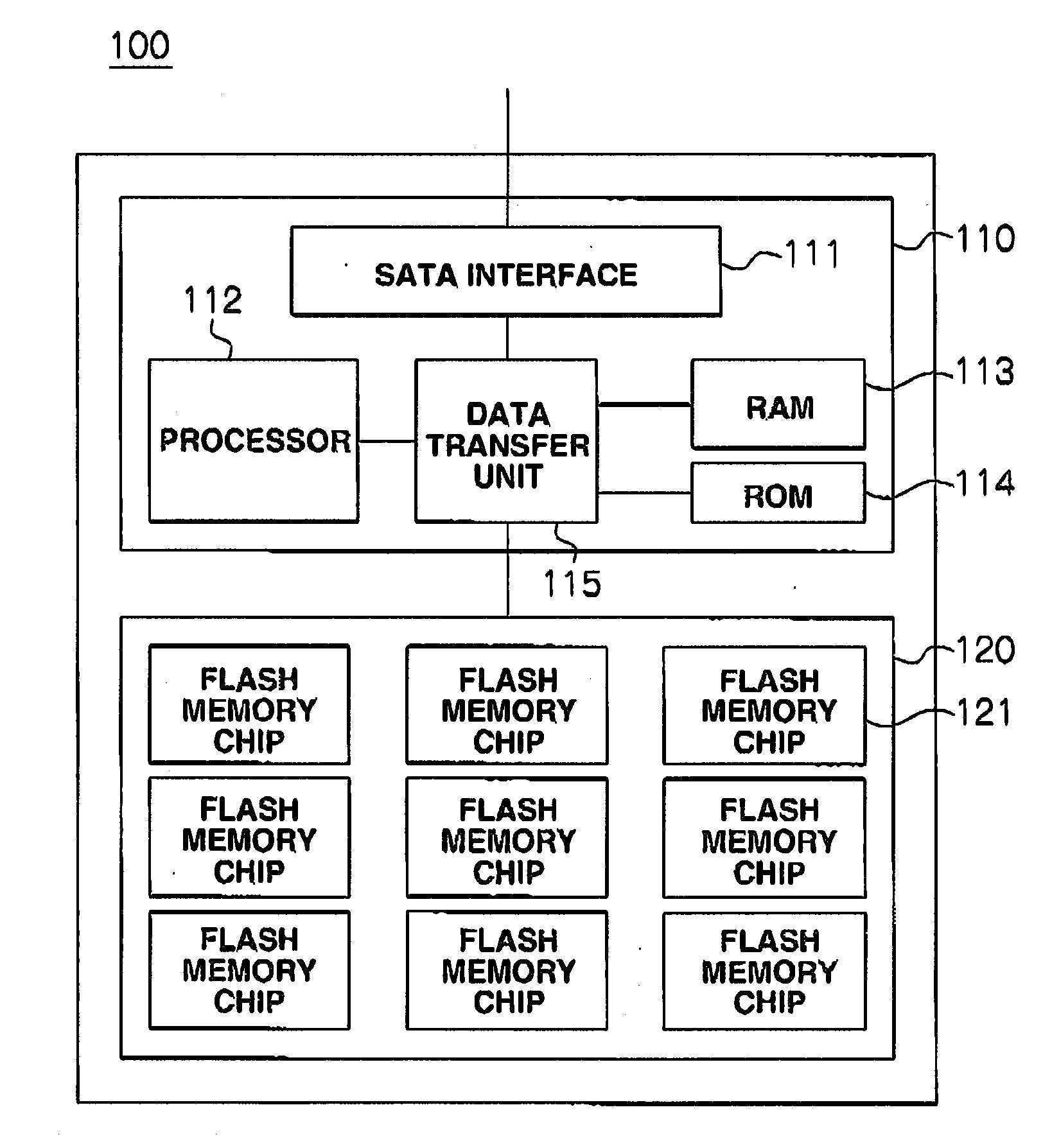
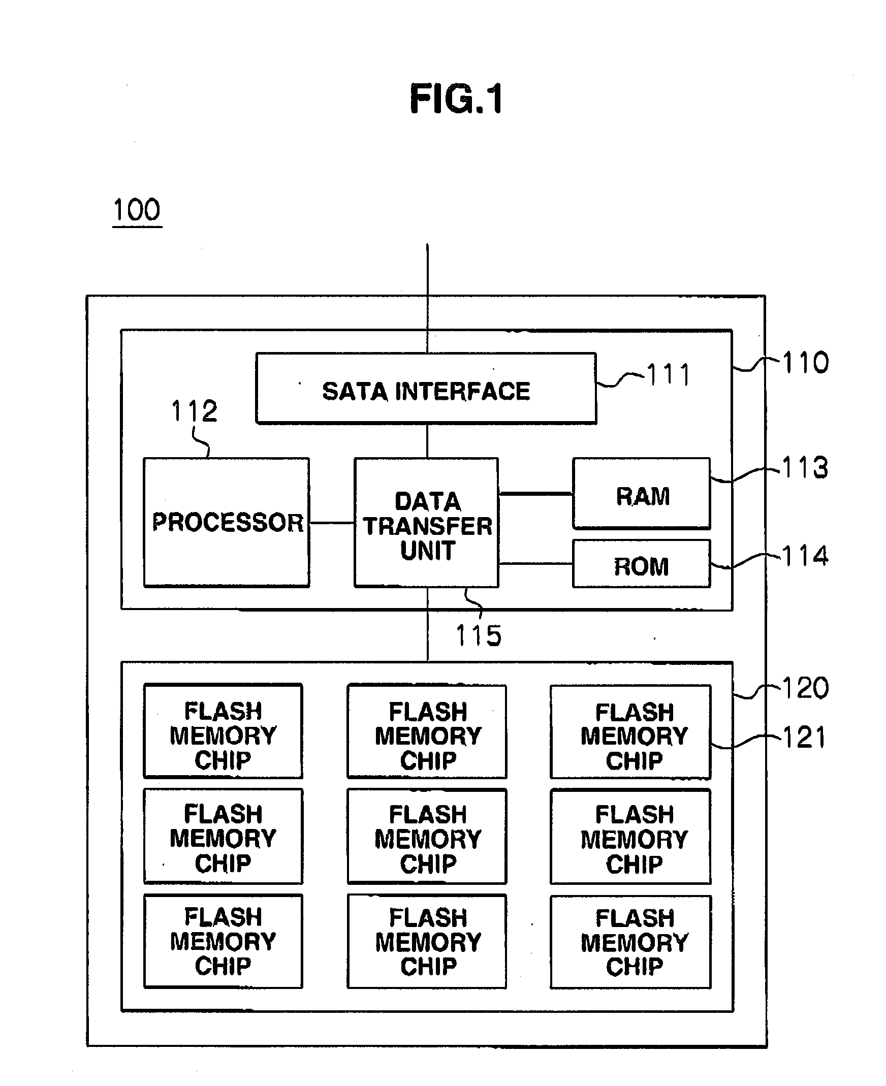
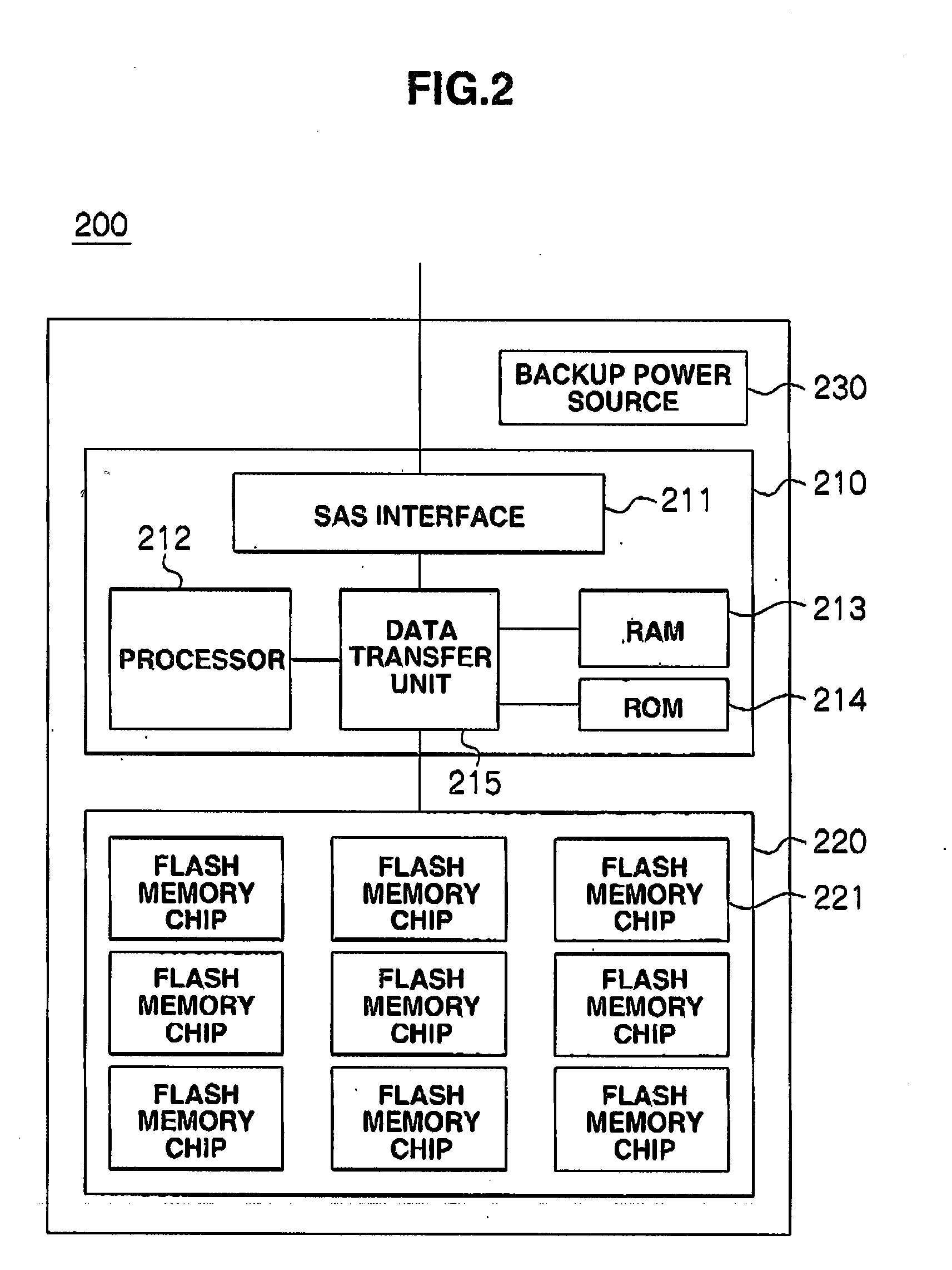
[0054]In the first embodiment, most (for example, 95%) SSD units employ a configuration formed with the C-SSD 100 connected to a SATA multiplexer 600 as shown in FIG. 6A (hereinafter referred to as “configuration A”), and the remaining few (for example, 5%) SSD units employ a configuration formed with the E-SSD 200 as shown in FIG. 6B (hereinafter referred to as “configuration B”). Every SSD unit of either configuration is made to participate in a redundant RAID group so that data stored in each SSD unit is protected. Incidentally, the SATA multiplexer 600 is an adapter apparatus that presents a one-port SATA interface as a two-port SATA interface in a pseudo manner.

[0055]In the first embodiment, the MPU PK 513 (or 523) executes write processing—basically performing substitute writing of data less than 64 KB, from among data to be written to the SSD units with configuration A, to the SSD units with configuration B, and then moving the plural pieces of data as a set from the SSD unit...

second embodiment

[0063]In the second embodiment, all the SSD units (such as 540-543 and 550-553) are configured as shown in FIG. 7 so that each of them is composed of the C-SSD 100, the E-SSD 200 with less capacity (for example, 5% in terms of capacity ratio) than the C-SSD 100, and an SSD adapter 700 connected to the C-SSD 100 and the E-SSD 200.

[0064]The SSD adapter 700 executes “reading” and “writing” of user data from and to each of the C-SSD 100 and the E-SSD 200. The SSD adapter 700 includes a processor 704, SATA interfaces 701, 702, a data transfer unit 7703, RAM 705, ROM 706, a SATA interface 707, and a SAS interface 708.

[0065]The data transfer unit 703 contains a bus logic and SAS and SATA control logics, and is connected to the other components 701, 702, 704-708. The processor 704 controls the data transfer unit 703 according to control firmware stored in the ROM 706. The RAM 705 functions as transfer data buffer memory and control firmware work memory. The data transfer unit 703 can accept...


PUM


Abstract

The size of a memory management unit in a low-performance non-volatile memory device is maintained, and the size of write data is compared with the size of the memory management unit. If the size of the write data is smaller than that of the memory management unit, the write data is cached by the high-performance non-volatile memory device; or if the size of the write data is not smaller, the write data is written to the low-performance device. Subsequently, a plurality of address values for the write data cached by the high-performance device are referred to; an address segment that is equal to the size of the memory management unit and in which the cached address values are consecutive; and data contained in that address segment is copied from the high-performance device to the low-performance device.

Description

CROSS-REFERENCES TO RELATED APPLICATIONS[0001]This application relates to and claims priority from Japanese Patent Application No. 2008-038176, filed on Feb. 20, 2008, the entire disclosure of which is incorporated herein by reference.BACKGROUND[0002]1. Field of the Invention[0003]The present invention relates to a storage system equipped with semiconductor storage apparatuses using electrically-rewritable non-volatile memory, and also to a data write method for such a storage system. More particularly, this invention relates to a storage system for storing data according to write performance characteristics of semiconductor storage apparatuses, and also relates to a data write method for such a storage system.[0004]2. Description of Related Art[0005]U.S. Pat. No. 7,136,973 discloses a method for enhancing write performance in a storage apparatus composed of two types of non-volatile devices with a difference in performance, Using that method, a specified amount of write data is cac...

Claims


Application Information

Patent Timeline
Patent Type & Authority Applications(United States)
IPC IPC(8): G06F12/00
CPCG06F2212/214G06F12/0866
Inventor MIZUSHIMA, NAGAMASA
Owner HITACHI LTD
Why Eureka
Try Eureka