Matrix Addressing Method and Circuitry and Display Device Using the Same

a technology of addressing circuit and matrix, applied in the field of matrix addressing circuitry, can solve the problems of extreme and achieve the effect of power saving and little degrading of image content legibility

Active Publication Date: 2009-08-27
INNOLUX CORP
View PDF5 Cites 44 Cited by
  • Summary
  • Abstract
  • Description
  • Claims
  • Application Information

AI Technical Summary

Benefits of technology

[0008]The invention has been made in view of the above problems, and its object is to provide a matrix addressing method and circuitry and display device, which enable power savings with as little degrading the legibility of content of an image as possible.

Problems solved by technology

However, in the method described in Patent Document 1, a displayed image is scaled down when decreasing the display area of the image that is an object to display, and so there is a risk of extremely degrading the legibility of content of the image.

Method used


Image

  • Matrix Addressing Method and Circuitry and Display Device Using the Same
  • Matrix Addressing Method and Circuitry and Display Device Using the Same
  • Matrix Addressing Method and Circuitry and Display Device Using the Same

Examples


embodiment 1

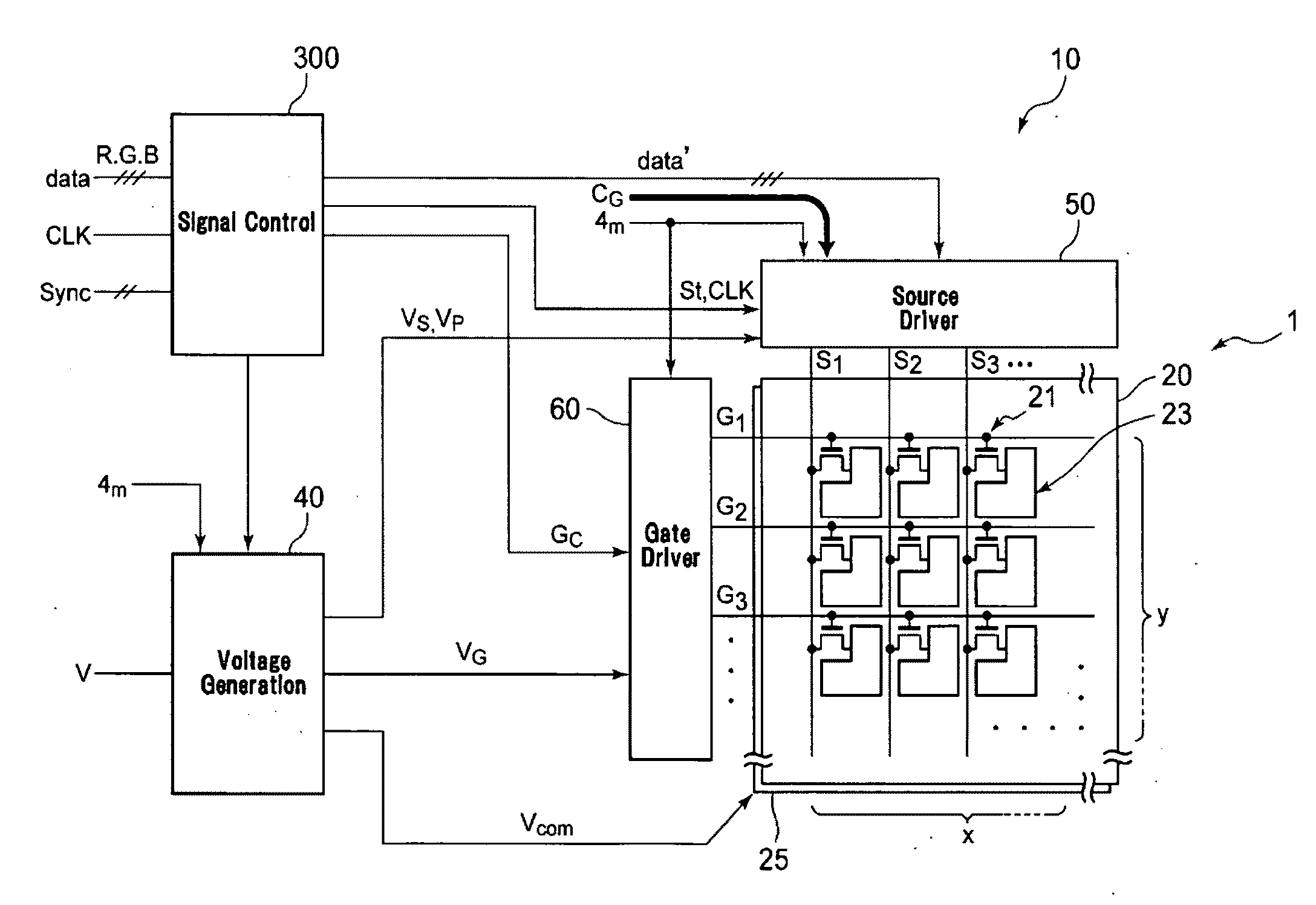
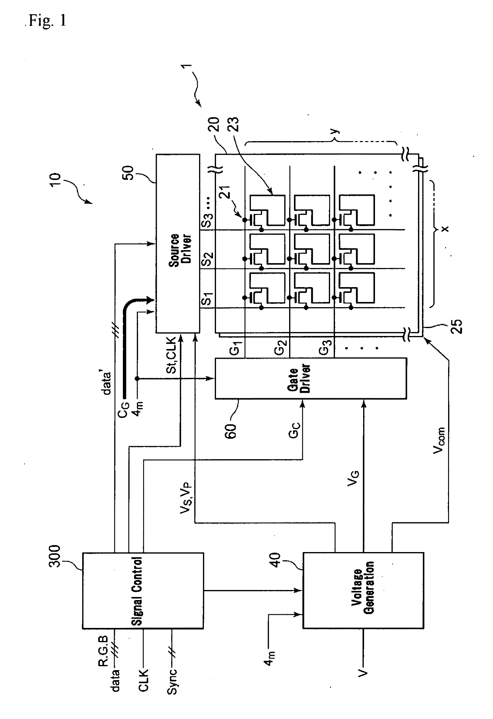
[0042]FIG. 1 illustrates a schematic basic configuration of a liquid crystal display device according to an embodiment of the invention.

[0043]In the figure, this liquid crystal display device is principally comprised of a liquid crystal display panel 1 of, for example, transmissive normally white mode, and peripheral circuitry for generating signals and voltages required to control and / or drive the panel 1 and supplying them to the panel.

[0044]The liquid crystal display panel 1 has a liquid crystal layer (not shown) perform optical modulation in accordance with an image to be displayed, the liquid crystal layer being sandwiched between two opposite transparent substrates. In this embodiment, the liquid crystal display panel 1 adopts an active matrix type structure, and on one substrate 20 on its rear side, for example, field-effect thin-film transistors (TFTs) 21 as pixel-driving active elements are arranged in matrix form corresponding to respective pixels in a predetermined displa...

embodiment 2

[0095]Described in the foregoing is the embodiment where the poor-gray-scale pixels are driven with two gray-scale voltages, the maximum voltage and the minimum voltage, in the power saving mode, and it is possible to represent totally eight colors by using two gray-scale voltages for each of R, G and B pixels. However, the number of driving voltages for the poor-gray-scale pixels are not limited to two as in the foregoing, and can be set at three or more without exceeding the number of gray-scale voltages in the normal mode.

[0096]FIG. 8 shows a gray-scale voltage generating circuit 2A according to the second embodiment, and includes a configuration to output three gray-scale voltages in the power saving mode, in addition to the configuration to output two-gray-scale voltages as shown in FIG. 4.

[0097]In this embodiment, in order to output not only the maximum and minimum gray-scale voltages #0 and #63 but also a voltage that is almost the middle of the voltages #0, #63 as a gray-sca...

embodiment 3

[0105]In the foregoing, switchover is made between driving of the rich-gray-scale pixels and driving of the poor-gray-scale pixels on a scanning-line basis, but it may be made on a pixel basis.

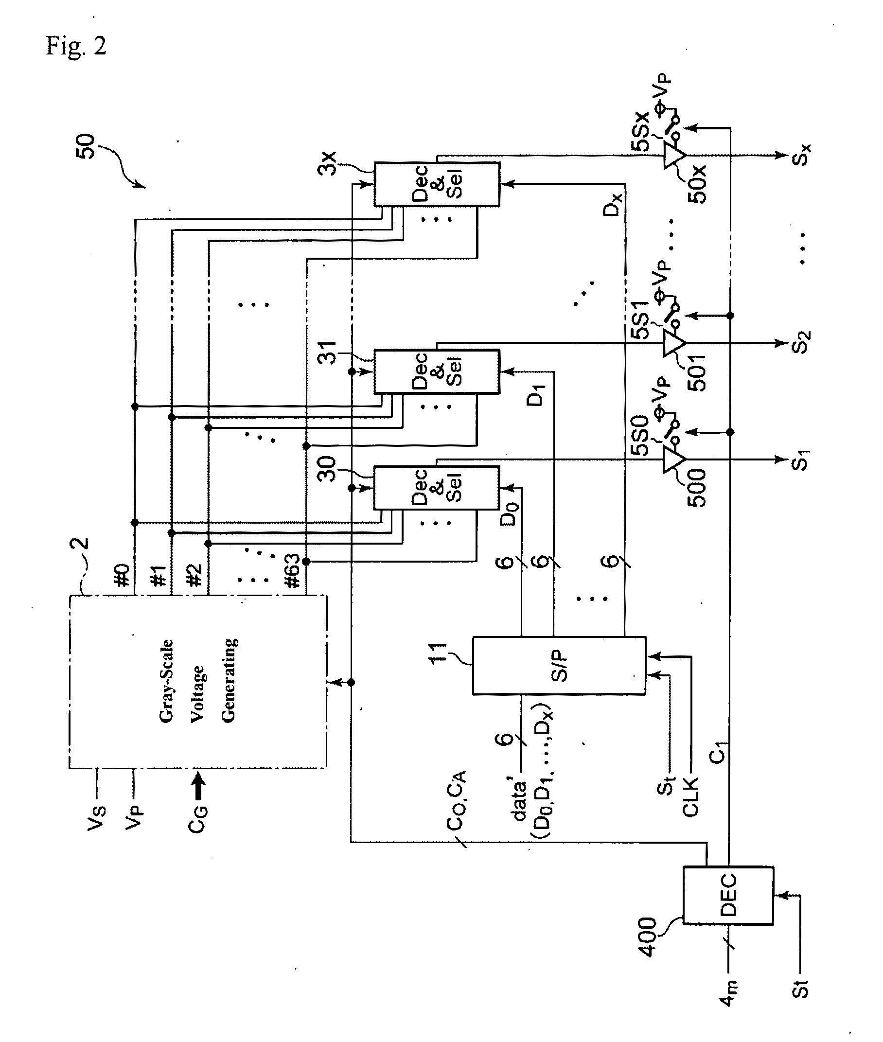
[0106]FIG. 9 illustrates a general configuration of a source driver 50B according to the third embodiment, where a modified mode decoder 400B generates control signals C00 to C0x including bits to individually control on / off the power supply control switches 5S1 to 5Sx of the buffer amplifiers in accord with the mode signal 4m. The control signals C00 to C0x are also supplied to the decoding selecting circuits 30 to 3x, respectively and have further bits to designate a selection state of gray-scale voltages in the decoding selecting circuits.

[0107]A gray-scale voltage generating circuit 2B used in the source driver SOB has the configuration shown in FIG. 4 without using the control signal C0 nor having all the switch circuits receiving the control signal C0 as their inputs, where the power sup...


PUM


Abstract

The invention aims at providing a matrix addressing method and circuitry and display device, which enable power savings without as little degrading the legibility of content of an image as possible. A matrix addressing method for driving pixels arranged over a display area by signals supplied to row electrodes and column electrodes arranged to cross one another. Rich-gray-scale pixel information signals (#0 to #63) are generated in a predetermined number of levels of gray scale according to original pixel information signals, while poor-gray-scale pixel information signals (#0 and #63) are generated in a smaller number of levels of gray scale than the maximum number of levels of gray scale, according to original pixel information signals, and rich-gray-scale pixels driven by the rich-gray-scale pixel information signals (#0 to #63) and poor-gray-scale pixels driven by the poor-gray-scale pixel information signals (#0 and #63) are mixed and coexist discretely in at least a part of the display area in a predetermined mixing pattern to display the same image object in a predetermined mode.

Description

BACKGROUND OF THE INVENTION[0001]1. Field of Invention[0002]The present invention relates broadly to a matrix addressing circuitry. The invention relates more particularly to a matrix addressing method and circuitry that drive row electrodes and column electrodes arranged to cross one another. The invention also relates to a display device using such addressing circuitry.[0003]2. Related Art[0004]Patent Document 1 discloses a method for displaying an image using a matrix display with image elements that radiate light in response to power supply, which comprises the steps of selecting a display mode from at least a first mode and a second mode, displaying an image on the display when the first mode is selected, and changing an image to display when the second mode is selected so that power consumption to display the image in the second mode is smaller than power consumption to display the image in the first mode. According to this method, power consumption is reduced in the second mo...

Claims


Application Information

Patent Timeline
Patent Type & Authority Applications(United States)
IPC IPC(8): G09G3/20
CPCG09G3/2011G09G3/2044G09G3/2051G09G3/3614G09G3/3688G09G3/3696G09G2340/0428G09G2310/027G09G2310/04G09G2320/0673G09G2330/021G09G2340/0407G09G2310/0213
Inventor HAGINO, SHUJIWATANABE, HIDETOSHIFURUI, YUKOIWATSU, AKIHIRO
Owner INNOLUX CORP
Why Eureka
Try Eureka