Manufaturing method of display device

a display device and manufacturing method technology, applied in the manufacture of electrode systems, electric discharge tubes/lamps, instruments, etc., can solve the problems of reducing the visibility and affecting the appearance of the display devi

Inactive Publication Date: 2009-08-27
PANASONIC LIQUID CRYSTAL DISPLAY CO LTD +1
View PDF5 Cites 35 Cited by
  • Summary
  • Abstract
  • Description
  • Claims
  • Application Information

AI Technical Summary

Benefits of technology

[0012]However, in the case of the configuration shown in FIG. 10, as the air layer is interposed in the space SP portion, a visibility may be re

Problems solved by technology

Consequently, an application step becomes complicated.
Furthermore, unless a height of the low viscosity adhesive is controlled with a high accuracy, a difference occurs in level between the low viscosity adhesive and the high viscosity adhesive, there is a possibility of larger air bubbles occurring.
Also, in the case of the technology described in JP-A-2005-243413, no des

Method used


Image

  • Manufaturing method of display device
  • Manufaturing method of display device
  • Manufaturing method of display device

Examples


embodiment 1

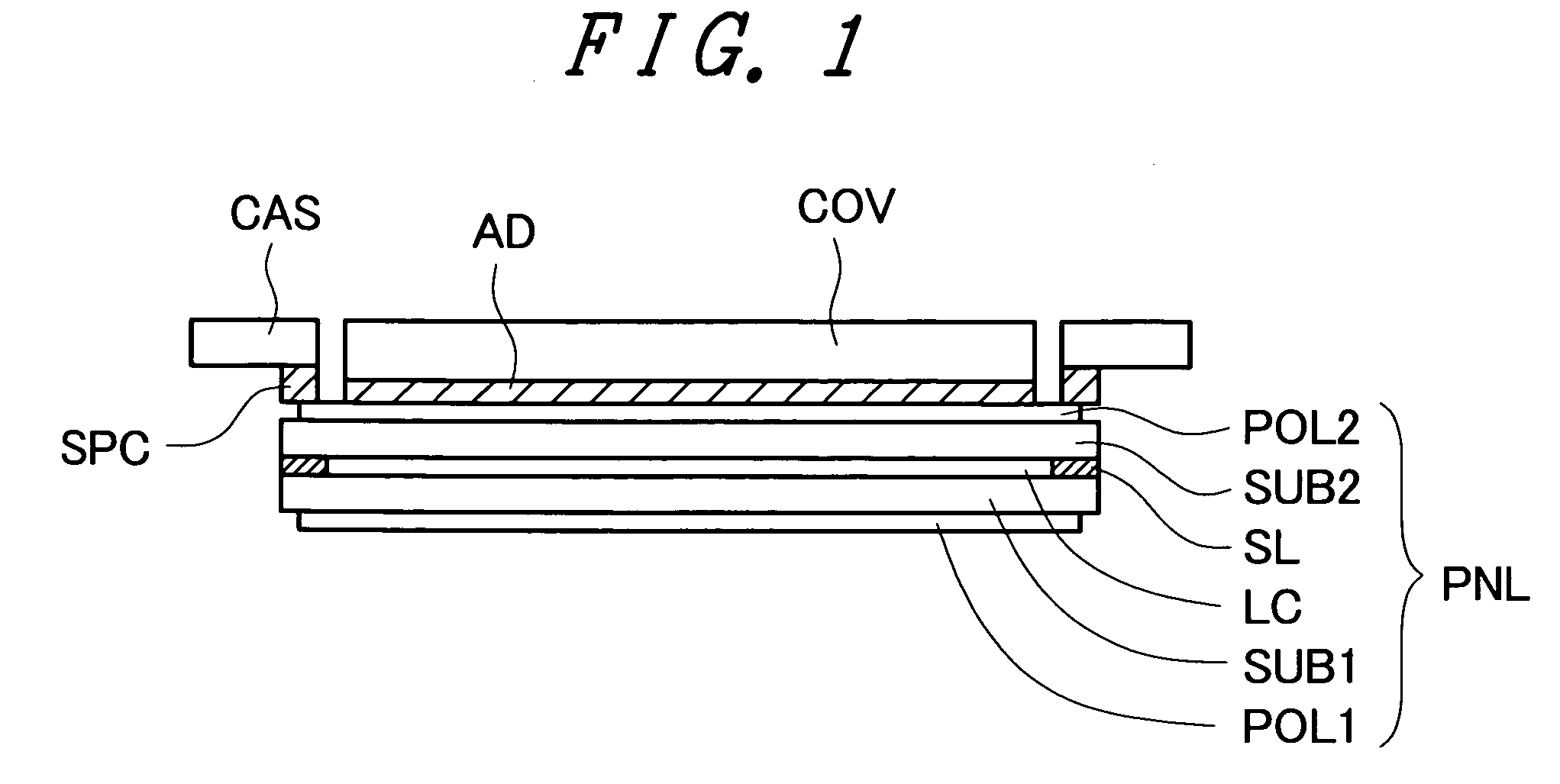
[0059]FIG. 1 is a sectional view illustrating one example of a display device of an embodiment 1 of the invention. In the embodiment 1, a description will be given exemplifying a case of using a liquid crystal display device as a display panel PNL. FIG. 1 also shows a condition in which a display panel PNL such as, for example, a liquid crystal display device is fitted on a casing CAS of a portable telephone or the like.

[0060]The display panel PNL has a substrate SUB1, which is a transmissive insulating substrate made of, for example, glass, a substrate SUB2, which is a transmissive insulating substrate made of, for example, glass, a seal material SL, which bonds the substrate SUB1 and the substrate SUB2 together, a liquid crystal LC sealed in within a portion surrounded by the substrate SUB1, the substrate SUB2, and the seal material SL, a polarizing plate POL1 disposed on a side of the substrate SUB1 opposite the liquid crystal LC, and a polarizing plate POL2 disposed on a side of...

embodiment 2

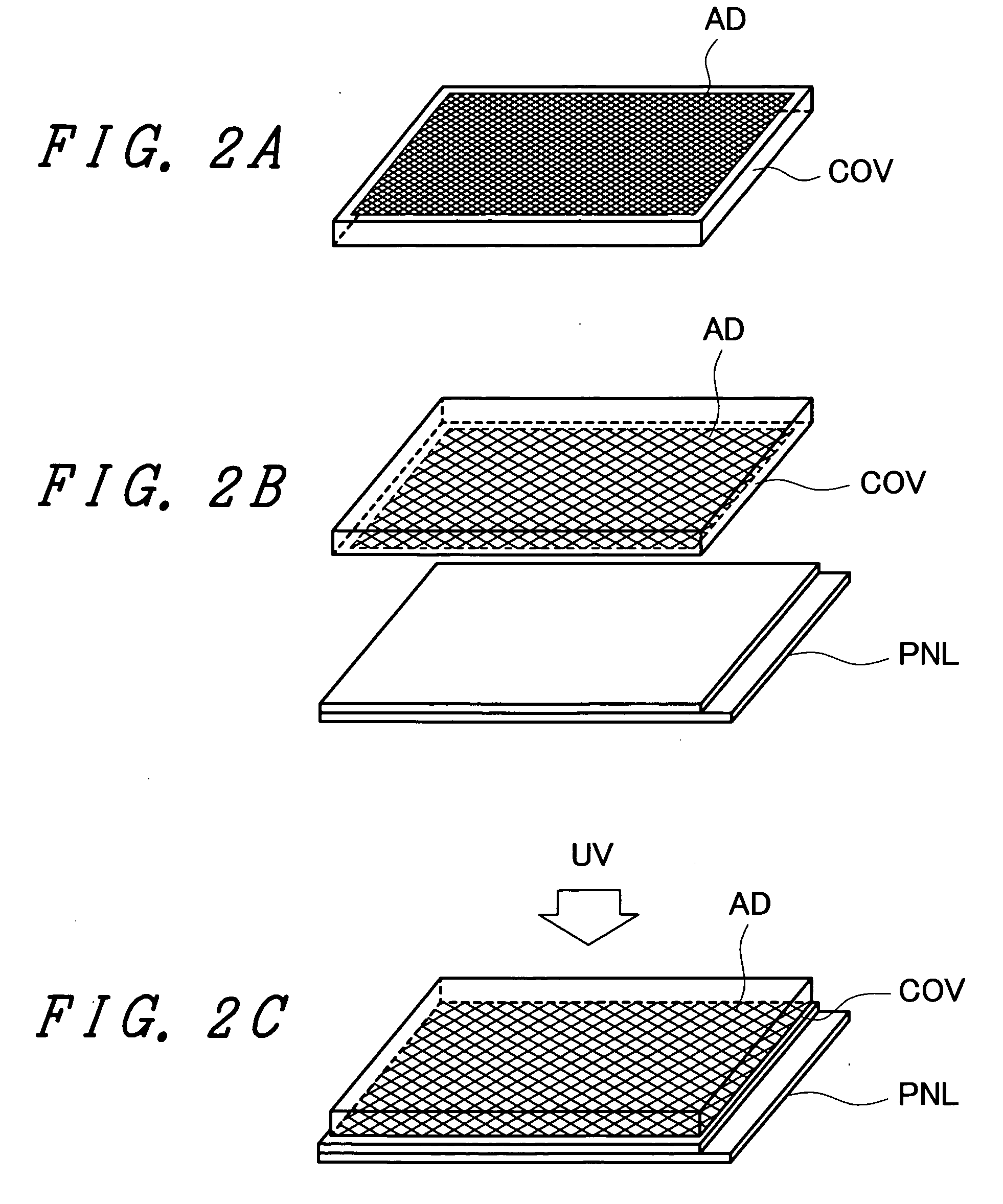
[0085]FIG. 6 is a side view illustrating one example of a method of manufacturing a display device of an embodiment 2 of the invention. When bonding the display panel PNL and the transparent substrate COV together, by their being bonded together while the display panel PNL is being bent in such a way as to be convex on a surface to be bonded, as shown in FIG. 6, it is possible to reduce a possibility of drawing in large air bubbles. In this case, it is desirable that a sum of a thickness t1 of the substrate SUB1 and a thickness t2 of the substrate SUB2 is 0.8 mm or less, more preferably, 0.6 mm or less. Although there is no particular restriction on a lower limit, it is desirable that the sum is 0.1 mm or more.

[0086]Although FIG. 6 shows an example in which the display panel PNL is being bent, this not being limiting, it is also acceptable that the display panel PNL and the transparent substrate COV are bonded together while only the transparent substrate COV, or both the display pa...

embodiment 3

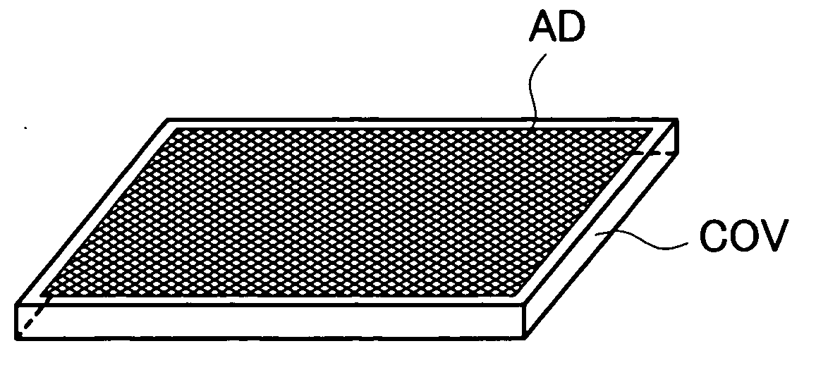
[0087]FIG. 7 is a sectional view illustrating one example of a display device of an embodiment 3 of the invention. A difference from FIG. 1 of the embodiment 1 is that the adhesive AD is extended to an extremity of the polarizing plate POL2. For example, by adjusting the viscosity, application pattern or application quantity of the adhesive AD, it is possible, at the time of the bonding, to spread the adhesive outside the extremity of the transparent substrate COV. Alternatively, by applying the adhesive AD to the display panel PNL side, too, it is possible to realize the invention.


PUM


Abstract

A method of manufacturing a display device in which a transparent substrate is bonded to a display panel by an adhesive, includes: applying the adhesive to the display panel or the transparent substrate in a predetermined pattern; bonding the display panel and the transparent substrate together by means of the adhesive after the applying step; and curing the adhesive after the bonding step, wherein in the applying step, a viscosity of the adhesive being more than 5000 mPa·s and 15000 mPa·s or less, the application of the adhesive is carried out by a screen printing, a time from a finishing point of the application of the adhesive in the applying step until a starting point of the bonding in the bonding step is 10 seconds or more and 120 seconds or less, in the bonding step, in a condition in which the adhesive applied in the applying step is spreading, with air bubbles remaining, and a maximum size of the air bubbles is 0.5 mm or less, the display panel and the transparent substrate are bonded together by the adhesive under a reduced pressure atmosphere lower than the atmospheric pressure, and in the curing step, after the maximum size of the air bubbles have reached 0.1 mm or less, ultraviolet light is applied, curing the adhesive.

Description

[0001]The present application claims priority from Japanese application JP 2008-39722 filed on Feb. 21, 2008, the content of which is hereby incorporated by reference into this application.BACKGROUND OF THE INVENTION[0002]1. Technical Field[0003]The present invention relates to a display device manufacturing method, and particularly, to a method of manufacturing a display device in which a transparent substrate (a protective cover) is bonded to a display panel by means of an adhesive.[0004]2. Related Art[0005]Display devices, such as liquid crystal display devices, are employed as display devices of various sizes from a small one for a portable telephone to a large one for a TV set.[0006]FIG. 10 is a sectional view illustrating a heretofore known liquid crystal display device. FIG. 10 shows a condition in which a display panel PNL such as, for example, a liquid crystal display panel is fitted on a casing CAS of a portable telephone or the like. In the case of the liquid crystal disp...

Claims


Application Information

Patent Timeline
IPC IPC(8): H01J9/20
CPCG02F1/133308G02F2202/28G02F2201/50G02F2001/13332G02F1/13332
Inventor KOBAYASHI, SETSUOMIWA, HIROAKIISHII, KATSUHIKO
Owner PANASONIC LIQUID CRYSTAL DISPLAY CO LTD
Why Eureka
Try Eureka