Supercharge Your Innovation With Domain-Expert AI Agents!

Layout design method of semiconductor integrated circuit

Inactive Publication Date: 2009-08-27
RENESAS ELECTRONICS CORP
View PDF21 Cites 2 Cited by
  • Summary
  • Abstract
  • Description
  • Claims
  • Application Information

AI Technical Summary

Benefits of technology

[0023]Moreover, the layout cell 100a has only one transistor defined by the channel region 103a. Therefore, it is possible to easily associate the layout cell 100a with the transistor. Similarly, the layout cell 100b has only one transistor defined by the channel region 103b. Therefore, it is possible to easily associate the layout cell 100b with the transistor. Consequently, it is possible to associate the transistor on the circuit diagram with the layout cells 100a and 100b on a one-to-two basis.
[0027]The exemplary aspect of the present invention facilitates creation of mapping information necessary for cross-probing.

Problems solved by technology

However, creating mapping information is difficult, and therefore a technology which facilitates mapping is required.
However, there is a problem that mapping information cannot be created by the method of Patent Document 1 when there is a cell including a plurality of elements on a layout (layout elements) corresponding to a single element on a circuit diagram.
Hence, it is not possible to create the mapping information associating the one transistor on the circuit diagram with the layout cell 100c on the one-to-one basis.

Method used


Image

  • Layout design method of semiconductor integrated circuit
  • Layout design method of semiconductor integrated circuit
  • Layout design method of semiconductor integrated circuit

Examples


Embodiment Construction

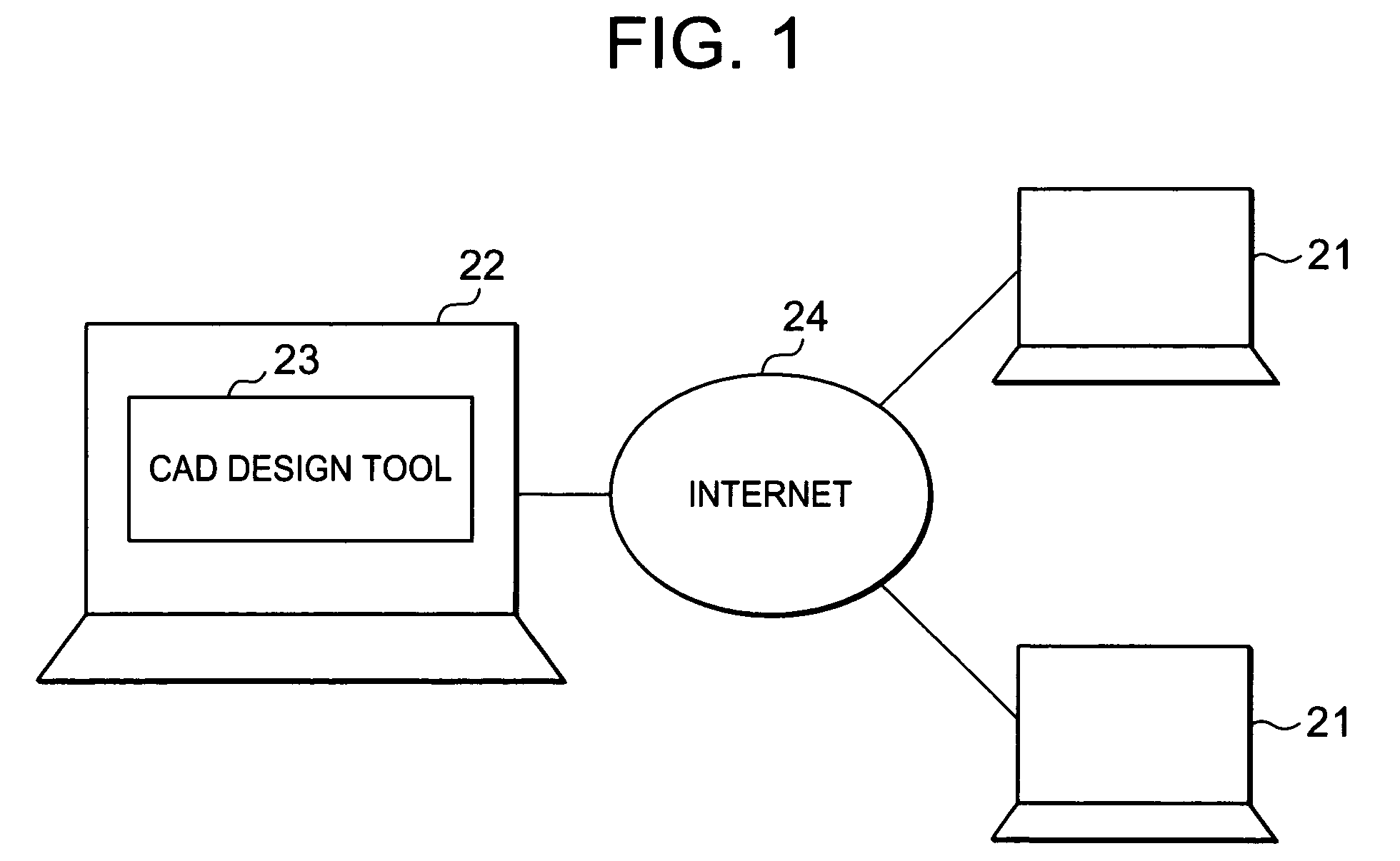
[0034]FIG. 1 is a system configuration diagram for carrying out an exemplary embodiment of the present invention. The system is configured of computer apparatuses 21, a server 22, a recording medium 23 and a network 24.

[0035]The recording medium 23 is held in the server 22 provided to offer an execution program, a model expression and a model parameter. The server 22 is connected to each of the computer apparatuses 21 such as an engineering workstation via the network 24 such as the Internet. A CAD design tool (a circuit editor, a layout editor, and the like) stored in the recording medium 23 is downloaded to the computer apparatus 21 via the network 24. The downloaded CAD design tool is stored in a local hard disk or memory of the computer apparatus 21.

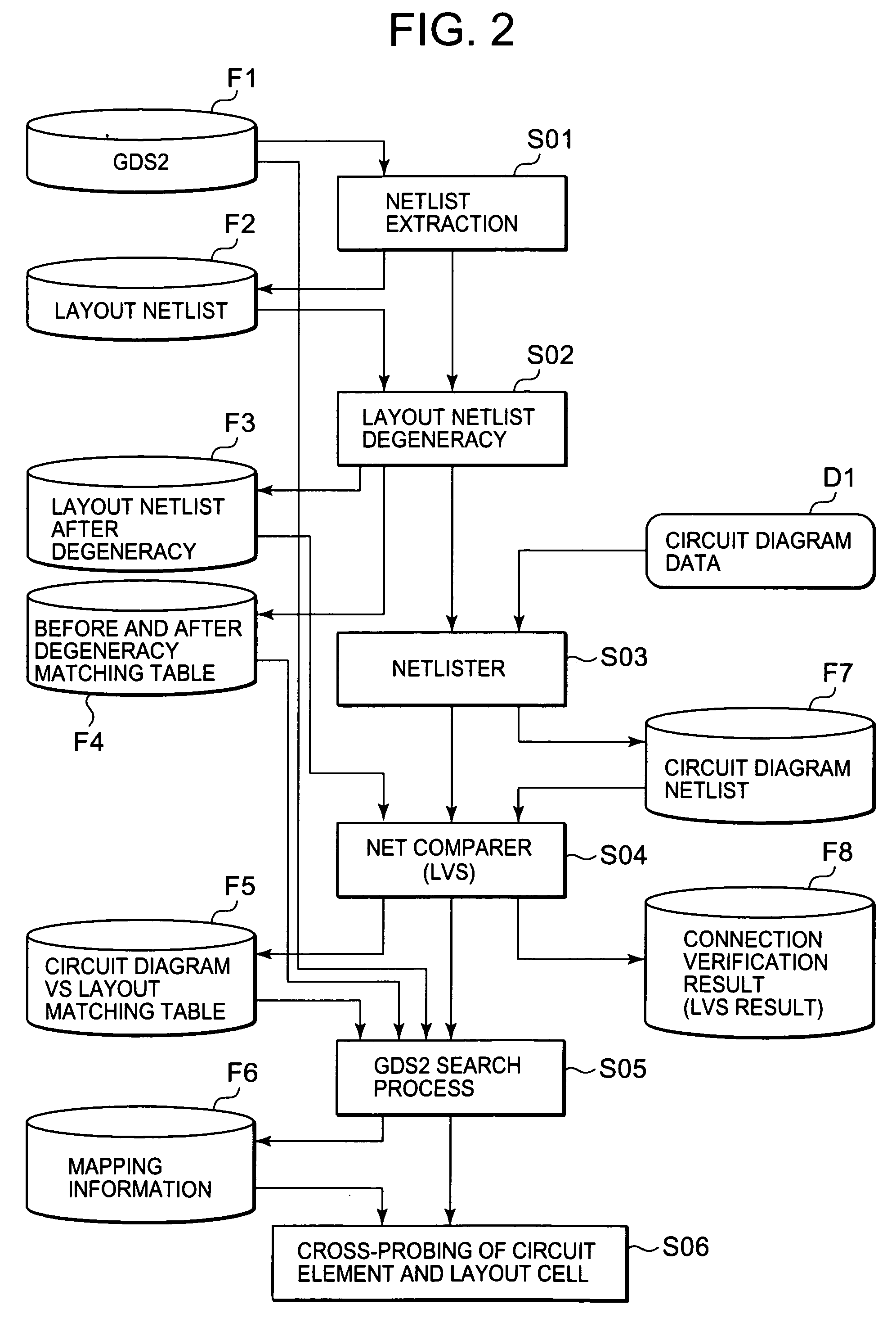
[0036]Next, descriptions will be given of a method for performing cross-probing between a circuit diagram and a layout according to the exemplary embodiment. FIG. 2 is a flowchart of cross-probing according to the exemplary embodimen...


PUM


Abstract

A layout design method of a semiconductor integrated circuit includes degenerating a layout netlist extracted from layout data, comparing the layout netlist after the reduction with a circuit diagram netlist, and creating a layout circuit association table of a layout cell after the reduction and a circuit element. The method includes creating a before and after reduction association table based on the layout netlist before and after the reduction, counting the number of layout elements in a layout cell area before the reduction, comparing the counted number of layout elements and the number of degenerated elements, and creating mapping information associating the layout cell with the circuit element.

Description

BACKGROUND OF THE INVENTION[0001]1. Field of the Invention[0002]The present invention relates to a layout design method of a semiconductor integrated circuit.[0003]2. Description of Related Art[0004]In recent years, an automation of analog layout design has progressed and a design period has been shortened. As a method of automating analog layout design, known is cross-probing that enables layout design while associating elements on a circuit diagram editor respectively with elements on a layout editor. Here, in order to perform layout design by cross-probing, it is necessary to create mapping information associating an element on the circuit diagram editor with a cell including an element on the layout editor.[0005]For example, when making design revision using already-existing layout data, the design is generally performed by reading a layout into a design system via a mask pattern file in a binary form typically used for storing layout information (hereinafter, referred to as GDS...

Claims


Application Information

Patent Timeline
IPC IPC(8): G06F17/50
CPCG06F17/5068G06F30/39
Inventor KOJIMA, MASAHIRO
Owner RENESAS ELECTRONICS CORP
Features
  • R&D
  • Intellectual Property
  • Life Sciences
  • Materials
  • Tech Scout
  • Unparalleled Data Quality
  • Higher Quality Content
  • 60% Fewer Hallucinations
Learn More