Semiconductor device
- Summary
- Abstract
- Description
- Claims
- Application Information
AI Technical Summary
Benefits of technology
Problems solved by technology
Method used
Image

Examples
Embodiment Construction
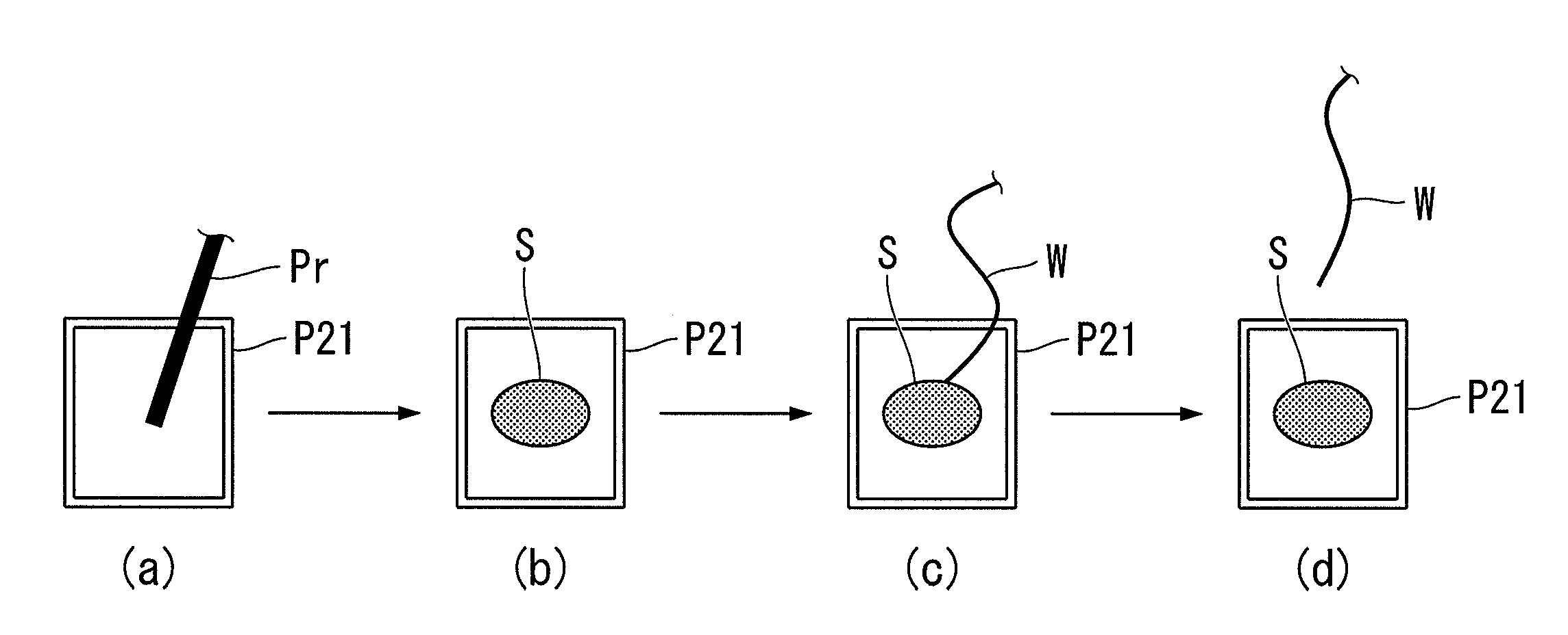
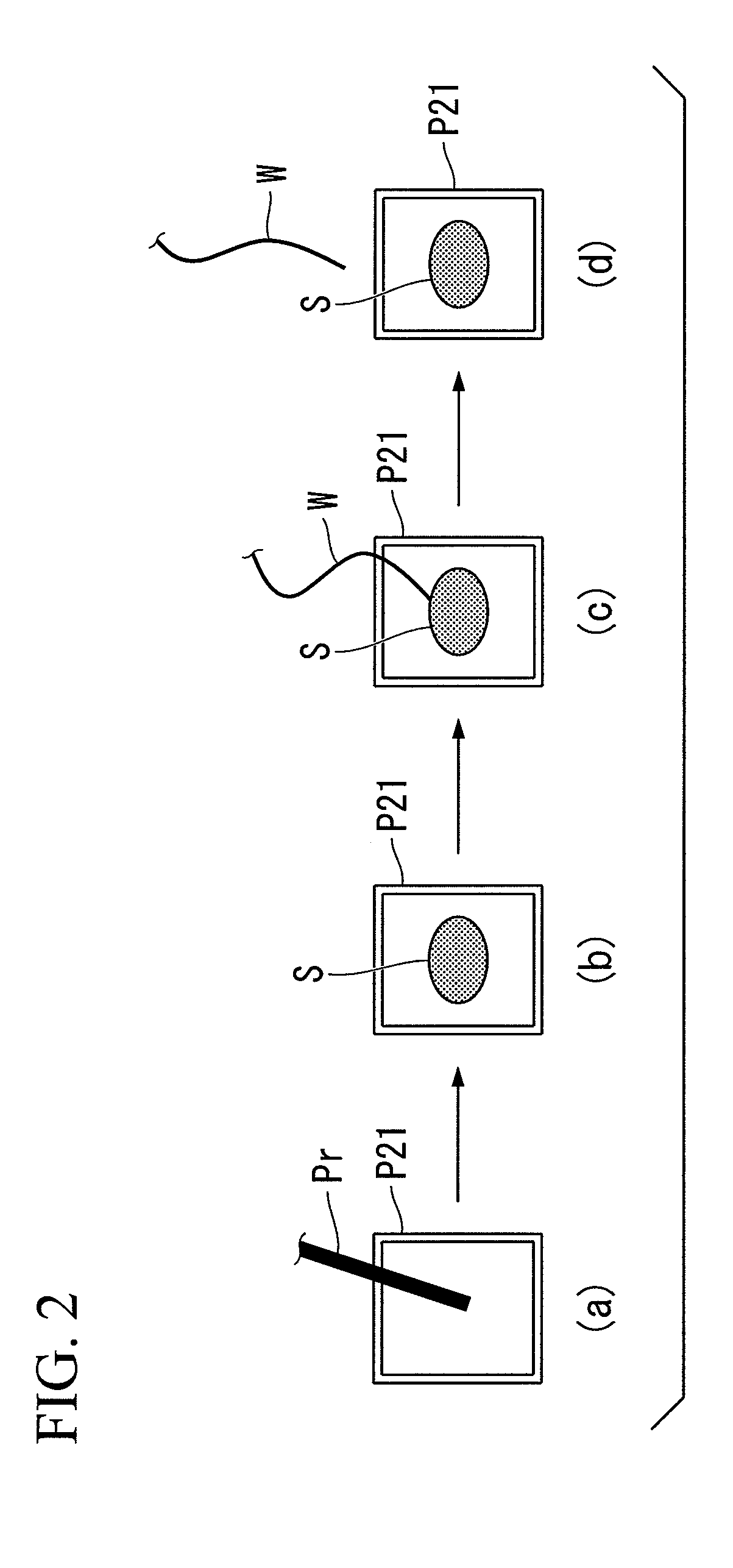
[0037]The invention will now be described herein with reference to illustrative embodiments. The accompanying drawings explain a semiconductor device and a method of manufacturing the semiconductor device in the embodiments, and the size, the thickness, and the like of each illustrated portion might be different from those of each portion of an actual semiconductor device.
[0038]Those skilled in the art will recognize that many alternative embodiments can be accomplished using the teachings of the present invention and that the invention is not limited to the embodiments illustrated herein for explanatory purposes.
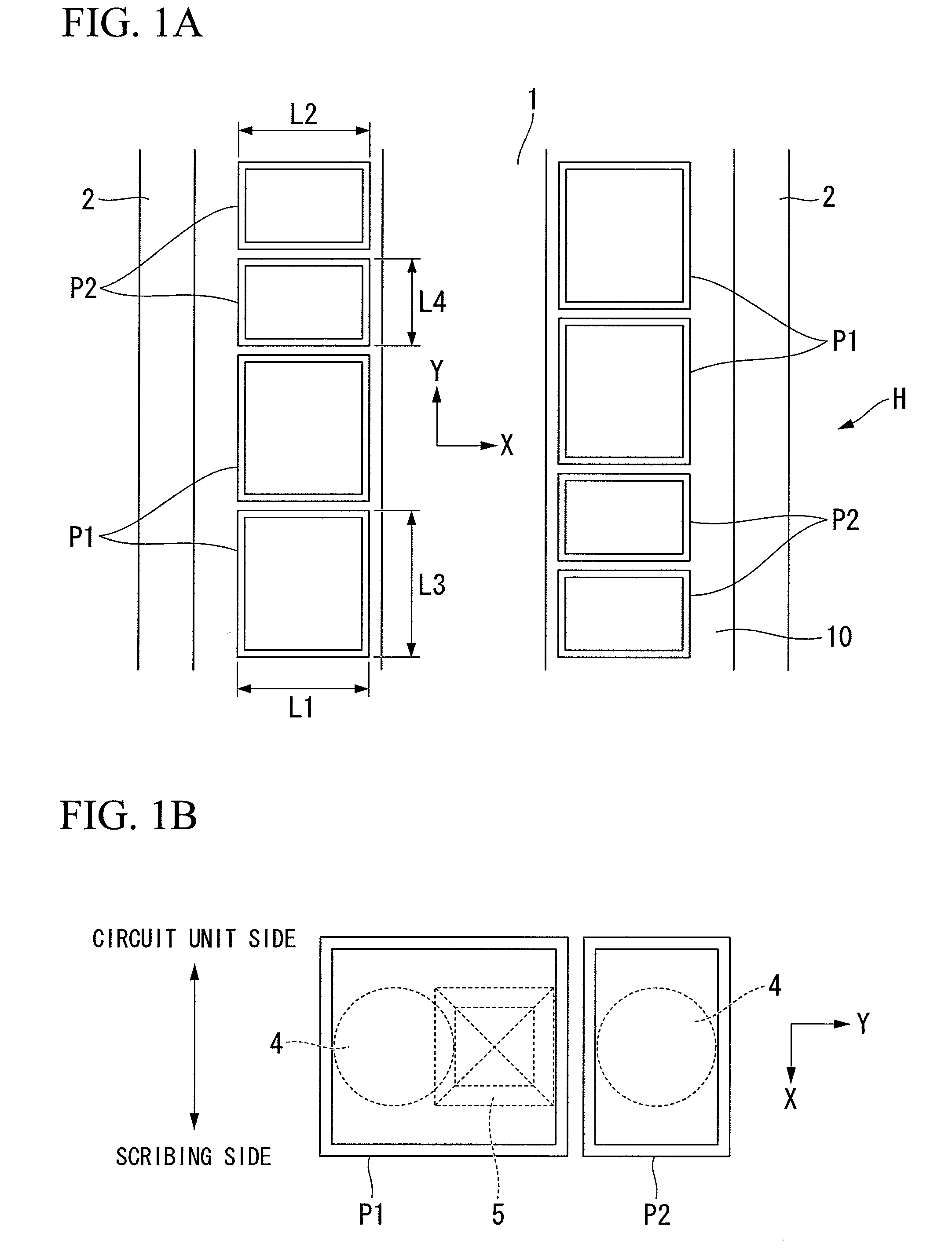
[0039]As shown in FIG. 1A, a semiconductor device H according to a first embodiment of the present invention mainly includes a semiconductor substrate 10, a circuit unit 1 provided on the semiconductor substrate 10, and multiple first and second pads P1 and P2 aligned in a line on both sides of the circuit unit 1. The pads P1 and P2 are connected to the circuit unit 1 throu...
PUM
 Abstract
Description
Claims
Application Information
 - Generate Ideas
- Intellectual Property
- Life Sciences
- Materials
- Tech Scout
- Unparalleled Data Quality
- Higher Quality Content
- 60% Fewer Hallucinations
Browse by: Latest US Patents, China's latest patents, Technical Efficacy Thesaurus, Application Domain, Technology Topic, Popular Technical Reports.
© 2025 PatSnap. All rights reserved.Legal|Privacy policy|Modern Slavery Act Transparency Statement|Sitemap|About US| Contact US: help@patsnap.com