Driving method of semiconductor device

a driving method and semiconductor technology, applied in static indicating devices, instruments, electroluminescent light sources, etc., can solve problems such as insufficient compensation of mobility, inability to accurately perform processes, and inability to reduce the influence of so as to reduce the influence of variation in current characteristics of transistors, and the effect of reducing the influence of variation in threshold voltage of transistors

Active Publication Date: 2009-09-10
SEMICON ENERGY LAB CO LTD
View PDF17 Cites 32 Cited by
  • Summary
  • Abstract
  • Description
  • Claims
  • Application Information

AI Technical Summary

Benefits of technology

[0069]The influence of variation in threshold voltage of a transistor can be reduced. Alternatively, the influence of variation in mobility of a transistor can be reduced. Alternatively, the influence of variation in current characteristics of a transistor can be reduced. Alternatively, a long input period of an image signal can be obtained. Alternatively, a long compensation period in order to reduce the influence of variation in threshold voltage can be obtained. Alternatively, a long compensation period to reduce the influence of variation in mobility can be obtained. Alternatively, a distortion of waveform of an image signal does not easily influence. Alternatively, not only the line sequential driving but also the dot sequential driving can be used. Alternatively, a pixel and a driver circuit can be formed over the same substrate. Alternatively, power consumption can be reduced. Alternatively, the cost can be reduced. Alternatively, a contact failure at a connection portion of wirings can be reduced. Alternatively, reliability can be increased. Alternatively, a large number of pixels can be increased. Alternatively, frame frequency can be increased. Alternatively, panel size can be increased.

Problems solved by technology

Therefore, various problems are caused.
As a result, accurate processes cannot be performed because of lack of process time, or compensation of mobility is insufficient because the period for compensation of variation in mobility is insufficient.
Therefore, input of an image signal to the pixel, compensation of variation in mobility, or the like cannot be performed sufficiently.
Accordingly, accurate compensation is impossible.

Method used


Image

  • Driving method of semiconductor device
  • Driving method of semiconductor device
  • Driving method of semiconductor device

Examples


embodiment mode 1

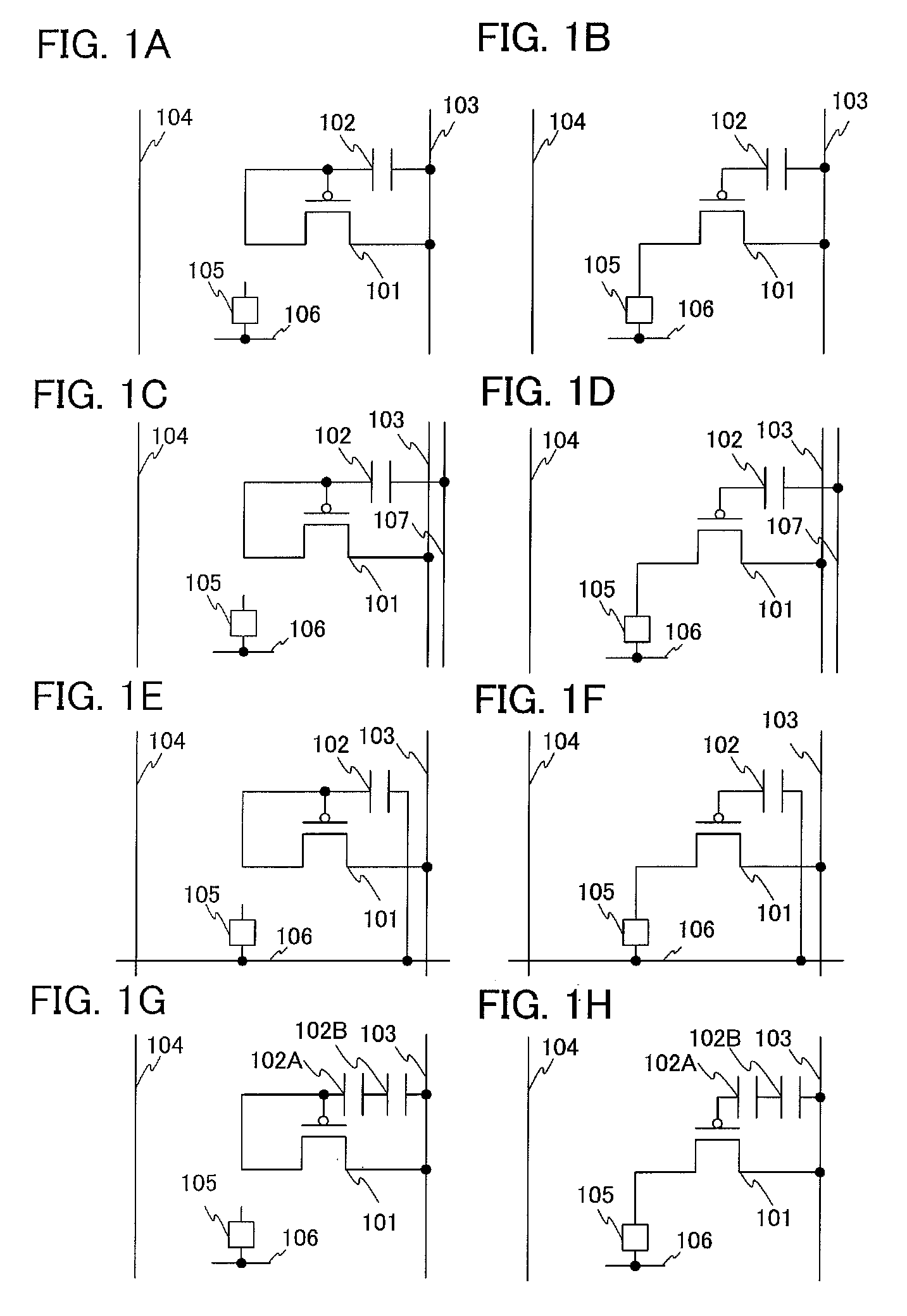
[0085]FIGS. 1A to 1H illustrate an example of a driving method, a drive timing, and a circuit configuration at the time in the case where variation in current characteristics such as mobility of a transistor is compensated.

[0086]FIG. 1A illustrates a circuit configuration in a period in which variation in current characteristics such as mobility of a transistor 101 is compensated. Note that the circuit configuration illustrated in FIG. 1A is the circuit configuration for discharging charge held in a gate of the transistor in order to compensate variation in current characteristics such as mobility of the transistor 101, and actually the relation of connection of the circuit configuration is realized by controlling on or off of a plurality of switches provided between wirings.

[0087]In FIG. 1A, a connection between a source (a drain, a first terminal, or a first electrode) of the transistor 101 and a wiring 103 is conducting. A connection between a drain (a source, a second terminal, ...

embodiment mode 2

[0135]This embodiment mode will describe a specific example of the circuit and a driving method described in Embodiment Mode 1.

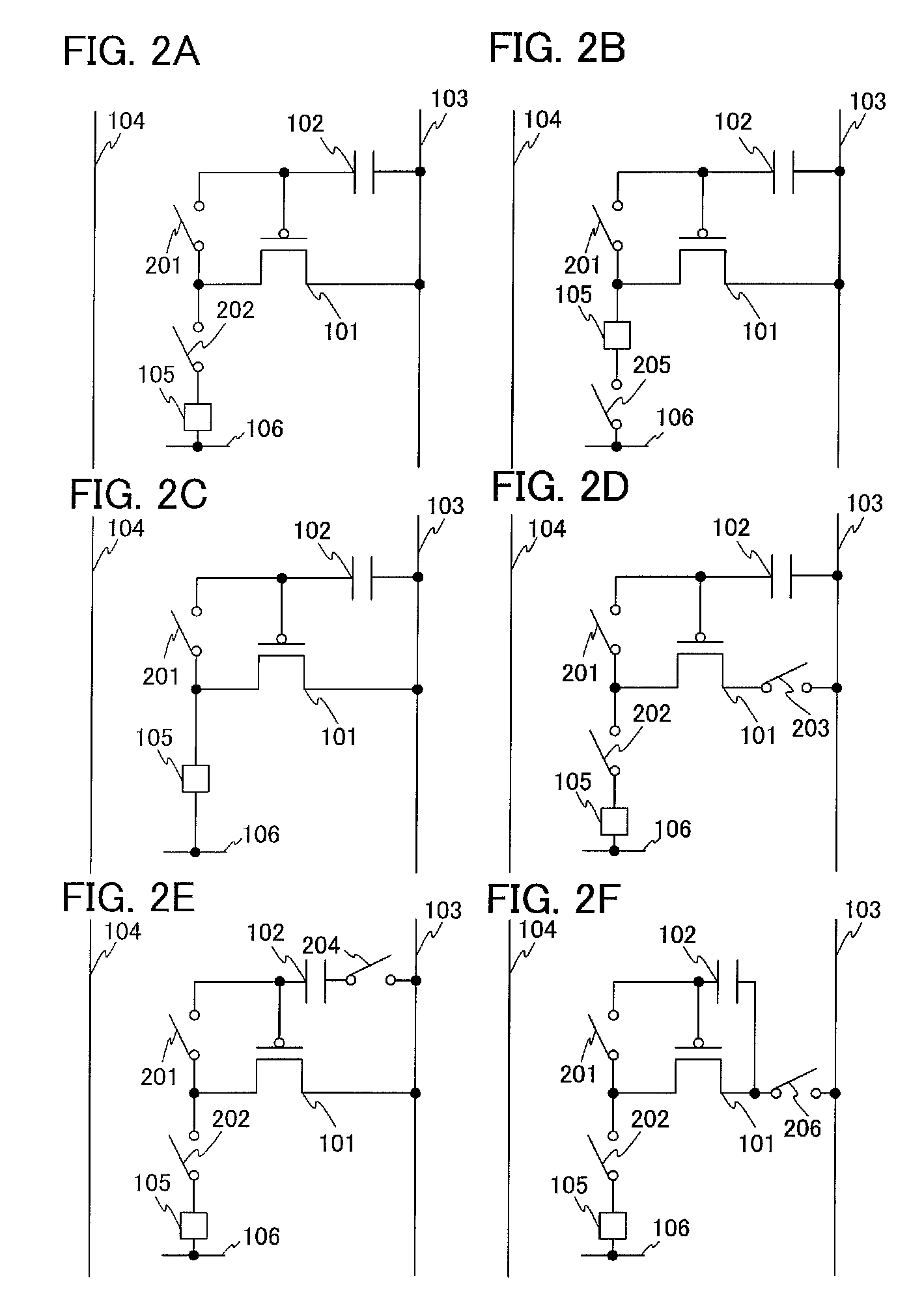
[0136]FIG. 6A illustrates a specific example of FIGS. 1A and 1B, and FIGS. 2A and 2D. A first terminal of a switch 601 is connected to the wiring 104, and a second terminal is connected to the source (or the drain) of the transistor 101. A first terminal of the switch 203 is connected to the wiring 103, and a second terminal is connected to the source (or the drain) of the transistor 101. The first terminal of the capacitor element 102 is connected to the gate of the transistor 101, and the second terminal is connected to the wiring 103. The first terminal of the switch 201 is connected to the gate of the transistor 101, the second terminal is connected to the drain (or the source) of the transistor 101. The first terminal of the switch 202 is connected to the drain (or the source) of the transistor 101, and the second terminal is connected to the first term...

embodiment mode 3

[0156]This embodiment mode will describe a specific example of the circuit and the driving method described in Embodiment Mode 1.

[0157]FIG. 9A illustrates a specific example of FIGS. 1A and 1B, and FIG. 2A. A first terminal of a switch 901 is connected to the wiring 104, and a second terminal is connected to the gate of the transistor 101. The first terminal of the capacitor element 102 is connected to the gate of the transistor 101, and the second terminal is connected to the wiring 103. The first terminal of the switch 201 is connected to the gate of the transistor 101, and the second terminal is connected to the drain (or the source) of the transistor 101. The first terminal of the switch 202 is connected to the drain (or the source) of the transistor 101, and the second terminal is connected to the first terminal of the display element 105. The second terminal of the display element 105 is connected to the wiring 106. The source (or the drain) of the transistor 101 is connected ...


PUM


Abstract

The semiconductor device includes a transistor and a capacitor element which is electrically connected to a gate of the transistor. Charge held in the capacitor element according to total voltage of voltage corresponding to the threshold voltage of the transistor and image signal voltage is once discharged through the transistor, so that variation in current flowing in the transistor or mobility of the transistor can be reduced.

Description

BACKGROUND OF THE INVENTION[0001]1. Field of the Invention[0002]The present invention relates to a semiconductor device or a driving method thereof.[0003]2. Description of the Related Art[0004]Flat panel displays such as liquid crystal displays (LCD) become widely used in recent years. However, the LCD has various drawbacks such as narrow viewing angle, narrow chromaticity range, slow response speed, and the like. Thus, as a display which overcomes those drawbacks, research of an organic EL (also referred to as an electroluminescence, an organic light-emitting diode, an OLED, or the like) display becomes active (see Patent Document 1).[0005]However, the organic EL display has a problem that current characteristics of a transistor for controlling current which flows to an organic EL element vary by pixels. When the current flowing to an organic EL element (in other words, current flowing to a transistor) varies, luminance of the organic EL element also varies, whereby a display scree...

Claims


Application Information

Patent Timeline
Patent Type & Authority Applications(United States)
IPC IPC(8): G09G3/30
CPCG09G3/3233G09G2320/043G09G2300/0819G09G3/20G09G3/30G09G3/32H05B33/12
Inventor KIMURA, HAJIME
Owner SEMICON ENERGY LAB CO LTD
Why Eureka
Try Eureka