

Method for driving semiconductor device
a technology of semiconductor devices and driving parts, applied in static indicating devices, instruments, television systems, etc., can solve problems such as insufficient mobility compensation, inability to perform accurate processes, and inability to reduce the influence of transistor current characteristics can be reduced, and influence of transistor threshold voltage variation can be reduced
- Summary
- Abstract
- Description
- Claims
- Application Information
AI Technical Summary
Benefits of technology
Problems solved by technology
Method used
Image

Examples
embodiment 1
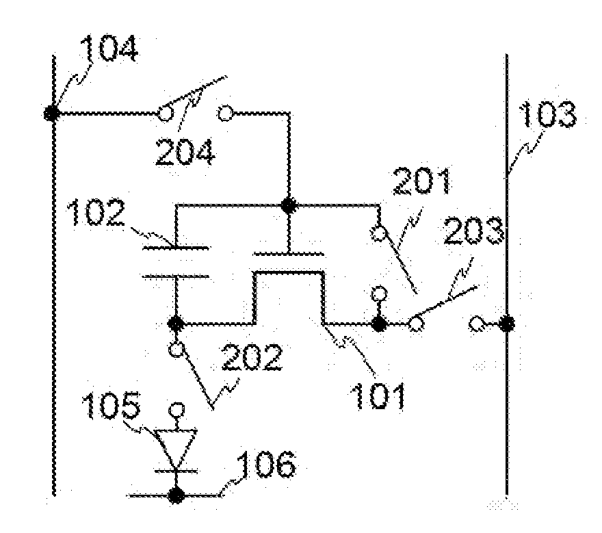
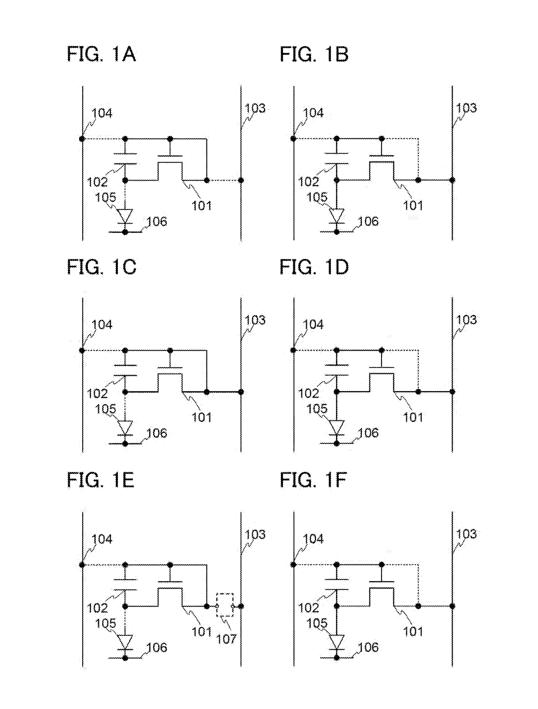
[0097]FIGS. 1A to 1F each illustrate an example of a driving method, drive timing, and a circuit configuration which are used when variation in current characteristics of transistors, such as mobility, is compensated. Note that in this embodiment, an n-channel transistor is described as an example.
[0098]FIG. 1A illustrates a circuit configuration in a period in which variation in current characteristics such as mobility of a transistor 101 is compensated. Note that the circuit configuration illustrated in FIG. 1A is a circuit configuration for discharging electric charge held in a gate of the transistor in order to compensate variation in current characteristics such as mobility of the transistor 101, and in practice, the connection relation in the circuit configuration is realized by controlling on and off of a plurality of switches provided between wirings. Note that in drawings, a solid line represents a conduction state between elements, and a dotted line represents a non-conduc...
embodiment 2
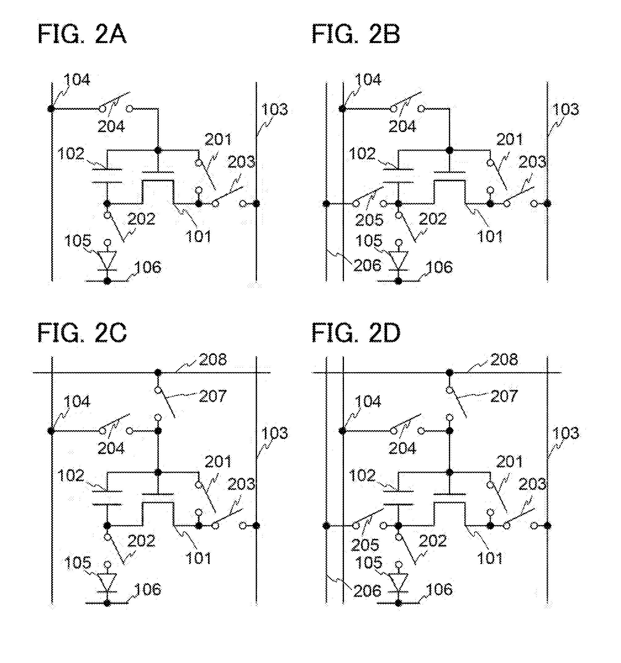
[0152]Next, in this embodiment, an application example of the circuit and the driving method which are described in Embodiment 1 will be described.
[0153]FIG. 7A illustrates a specific example of FIGS. 1A and 1B. The first terminal of the switch 201 is electrically connected to the gate of the transistor 101 and the first terminal of the capacitor 102. The second terminal of the switch 201 is electrically connected to the first terminal of the transistor 101. Moreover, the first terminal of the switch 202 is electrically connected to the second terminal of the transistor 101 and the second terminal of the capacitor 102. The second terminal of the switch 202 is electrically connected to the first terminal of the display element 105. Further, the first terminal of the switch 203 is electrically connected to the wiring 103. The second terminal of the switch 203 is electrically connected to the first terminal of the switch 201, the gate of the transistor 101, and the first terminal of th...
embodiment 3
[0171]Next, in this embodiment, an application example of the circuit and the driving method which are described in Embodiment 1 will be described.
[0172]FIG. 11A illustrates a specific example of FIGS. 1C and 1D. A first terminal of a switch 301 is electrically connected to the wiring 103. A second terminal of the switch 301 is electrically connected to the gate of the transistor 101 and the first terminal of the capacitor 102. The first terminal of the switch 202 is electrically connected to the second terminal of the transistor 101 and the second terminal of the capacitor 102. The second terminal of the switch 202 is electrically connected to the first terminal of the display element 105. Further, a first terminal of a switch 303 is electrically connected to the wiring 103. A second terminal of the switch 203 is electrically connected to the first terminal of the transistor 101. The first terminal of the switch 204 is electrically connected to the second terminal of the switch 301...
PUM
 Abstract
Description
Claims
Application Information