Surface mounted piezoelectric vibrator

a piezoelectric and surface mounted technology, applied in piezoelectric/electrostrictive/magnetostrictive devices, oscillator generators, semiconductor/solid-state device details, etc., can solve the problems of easy adverse effects, electromagnetic waves thus radiated, and adverse effects on piezoelectric vibration element signals, so as to prevent unwanted radiation (radiation noise) and easy adverse effects

Active Publication Date: 2017-11-28
DAISHINKU CORP
View PDF27 Cites 15 Cited by
  • Summary
  • Abstract
  • Description
  • Claims
  • Application Information

AI Technical Summary

Benefits of technology

[0036]In addition to the advantageous effects described above, by thus forming the third internal terminal pads and the wiring patterns that respectively extend the third internal terminal pads on the same surface along a part of perimeter of the first internal terminal pads, the first internal terminal pads electrically connected to the piezoelectric vibration element can be isolated from the second internal terminal pads, in one of which is the AC output is included, by the third internal terminal pads and the associated wiring patterns formed on the same surface. By virtue of this structural advantage, any radiation noise generated by high frequency signals and / or alternating current flowing through one of the second internal terminal pads is blocked by the conductive paths formed by the third internal terminal pads and the wiring patterns that respectively extend the third internal terminal pads. The radiation noise, most of which is thus blocked, hardly arrives at the first internal terminal pads formed on the same surface and connected to the piezoelectric vibration element easily adversely affected by the noise. This successfully prevents unwanted radiation (radiation noise) generated by the AC output of the second internal terminal pad from adversely affecting the piezoelectric vibration element electrically connected to the first internal terminal pads.
[0037]Conventionally, the piezoelectric vibrators undergo the occurrence of phase differences and potential differences due to different signal waveforms between signals flowing through the AC output in one of the second internal terminal pads and signals flowing through the first internal terminal pads connected to the piezoelectric vibration element although these signals have the same frequency. These phase and current differences may prompt interactions between the AC output of the second internal terminal pad and the first internal terminal pads, possibly resulting in operational problems. On the other hand, the invention controls any operational problems caused by such interactions because the first internal terminal pads electrically connected to the piezoelectric vibration element are shut off from the second internal terminal pads in one of which the AC output is included by the conductive paths formed by the third internal terminal pads and the wiring patterns that respectively extend the third internal terminal pads on the same plane.
[0038]According to a fourth aspect of the invention, in addition to the technical features described above, the piezoelectric vibrator is preferably characterized in that the piezoelectric vibration element is an AT-cut crystal piece.
[0039]According to a fifth aspect of the invention, in addition to the technical features described above, the piezoelectric vibrator is preferably characterized in that the base includes a bottom portion constituting a lowermost layer, a first bank portion constituting a middle layer, and a second bank portion constituting an uppermost layer, the bottom portion constituting the lowermost layer is constructed of a single plate made of a ceramic material and having a rectangular shape in plan view, the first bank portion constituting the middle layer is made of a ceramic material and formed in a frame shape in plan view on the bottom portion constituting the lowermost layer, the second bank portion constituting the uppermost layer is made of a ceramic material and formed in a frame shape in plan view on the first bank portion constituting the middle layer,
[0040]the housing portion of the base corresponding to the lowermost layer includes a first housing portion formed by the first bank portion constituting the middle layer to house therein the integrated circuit element, and a second housing portion formed by the second bank portion constituting the uppermost layer to house therein the piezoelectric vibration element, and the plurality of internal terminal pads are formed on an inner bottom surface of the first housing portion.
[0041]According to a sixth aspect of the invention, in addition to the technical features described above, the piezoelectric vibrator is preferably characterized in that the base includes an intermediate plate portion constituting a middle layer, a third bank portion constituting an upper layer, and a fourth bank portion constituting a lower layer, the intermediate plate portion constituting the middle layer is constructed of a single plate made of a ceramic material and having a rectangular shape in plan view, the third bank portion constituting the upper layer is made of a ceramic material and formed on the intermediate plate portion constituting the middle layer, the fourth bank portion constituting the lower layer is made of a ceramic material and formed in a frame shape in plan view below the intermediate plate portion constituting the middle layer, the housing portion of the base includes a third housing portion formed by the third bank portion constituting the upper layer to house therein the piezoelectric vibration element, and a fourth housing portion formed by the fourth bank portion constituting the lower layer to house therein the integrated circuit element, and the first to third internal terminal pads are formed on an inner bottom surface of the fourth housing portion.

Problems solved by technology

When such a piezoelectric vibrator is miniaturized, its operation is easily adversely affected by unwanted radiation (hereinafter, called radiation noise) generated by alternating current signals and / or high frequency signals flowing from the internal terminal pad for output of the base connected to the output pad of the integrated circuit element (which corresponds to the signal output unit P3 illustrated in FIG. 10) to the wiring patterns for output (signal output units of the integrated circuit element).
These phase and current differences may prompt interactions between the integrated circuit element signals and the piezoelectric vibration element signals, possibly resulting in operational problems.
The electromagnetic wave thus radiated may adversely affect the piezoelectric vibration element signals which are vibration sources.

Method used


Image

  • Surface mounted piezoelectric vibrator
  • Surface mounted piezoelectric vibrator
  • Surface mounted piezoelectric vibrator

Examples


Embodiment Construction

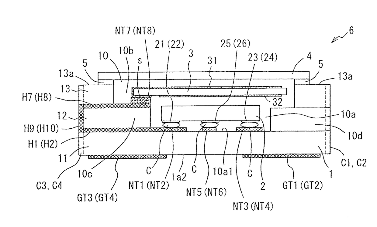
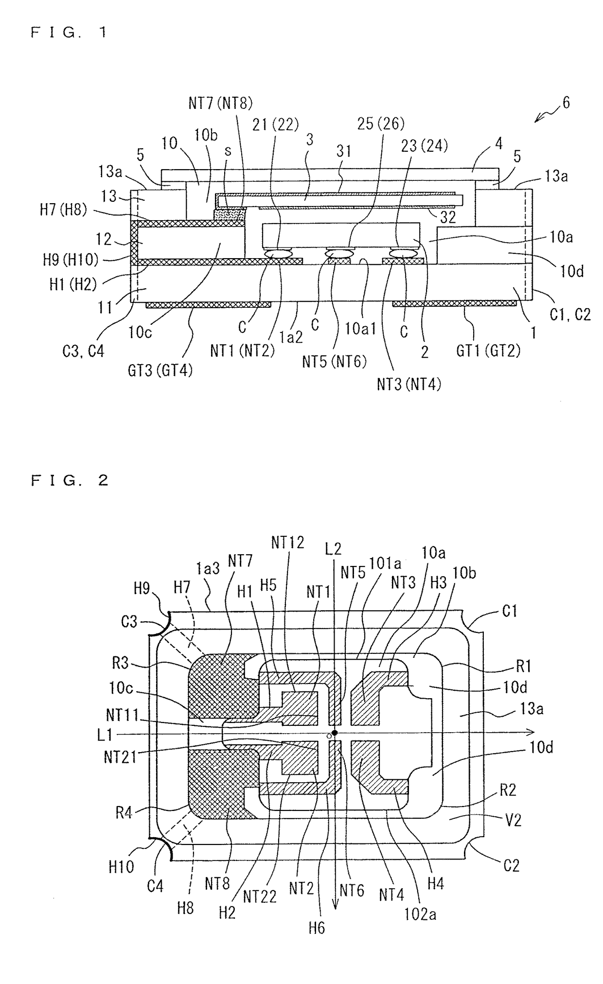
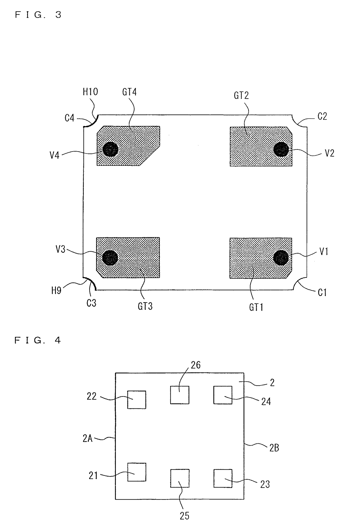
[0055]Hereinafter, examples of a piezoelectric vibrator according to the invention are described referring to the accompanying drawings. FIGS. 1 to 3 are drawings of a first example of the invention. FIG. 4 is a bottom view of an integrated circuit element to which the invention is applied. FIGS. 5 and 6 are drawings of a second example of the invention. FIG. 7 is a drawing of a third example of the invention. FIG. 8 is a drawing of a fourth example of the invention. FIG. 9 is a drawing of a fifth example of the invention. In these examples, the same reference symbols are consistently used for any common or corresponding structural elements. In these examples, a crystal vibrator is used as a piezoelectric vibrator.

[0056]The first example is described referring to FIGS. 1 to 4

[0057]A crystal vibrator 6 includes a base 1 having a recessed portion, an integrated circuit element 2 housed in a lower section of the recessed portion of the base 1, a piezoelectric vibration element 3 housed...


PUM


Abstract

A piezoelectric vibrator according to the invention has a base, an integrated circuit element, and a piezoelectric vibration element. The base has internal terminal pads, and external terminals including an AC output terminal. The base includes rectangular ceramic substrate layers stacked in at least three layers, each of which has castellations formed at four corners. Among the internal terminal pads, internal terminal pads for the integrated circuit element and internal terminal pads for the piezoelectric vibration element are connected to each other by externally exposed wiring patterns formed on upper surfaces of the castellations at the corners of the ceramic substrate constituting a middle layer.

Description

BACKGROUND OF THE INVENTION[0001]The invention relates to surface mounted piezoelectric vibrators structurally characterized in that a package is constructed of a base having an opening on its upper-surface side and a housing portion formed in its interior, and a cover that seals the opening, and a piezoelectric vibration element and an integrated circuit element are housed in the housing portion of the base (hereinafter, simply referred to as “piezoelectric vibrator”). The invention more particularly relates to improvements in such package constructions of the piezoelectric vibrators.[0002]Very accurate vibratory frequencies can be constantly obtained with the piezoelectric vibrators in which piezoelectric vibration elements, for example, crystal pieces, are used. Such piezoelectric vibrators are, therefore, conventionally employed in diverse fields as reference frequency sources for electronic devices. The piezoelectric vibrators typically have a structure in which an integrated c...

Claims


Application Information

Patent Timeline
Patent Type & Authority Patents(United States)
IPC IPC(8): H01L41/053H03H9/10H03H9/17H01L41/047H03H9/05H03B5/36H01L23/00
CPCH01L41/053H01L41/0475H03B5/364H03H9/0547H03H9/0552H03H9/0561H03H9/1021H03H9/17H03H9/171H01L2924/3025H01L2924/12042H01L2924/00014H01L2224/81207H01L24/13H01L24/16H01L24/48H01L24/81H01L24/85H01L2224/13144H01L2224/16225H01L2224/16227H01L2224/48227H01L2924/00H01L2224/45099H01L2224/45015H01L2924/207H10N30/88H10N30/875
Inventor KOJO, TAKUYA
Owner DAISHINKU CORP
Why Eureka
Try Eureka