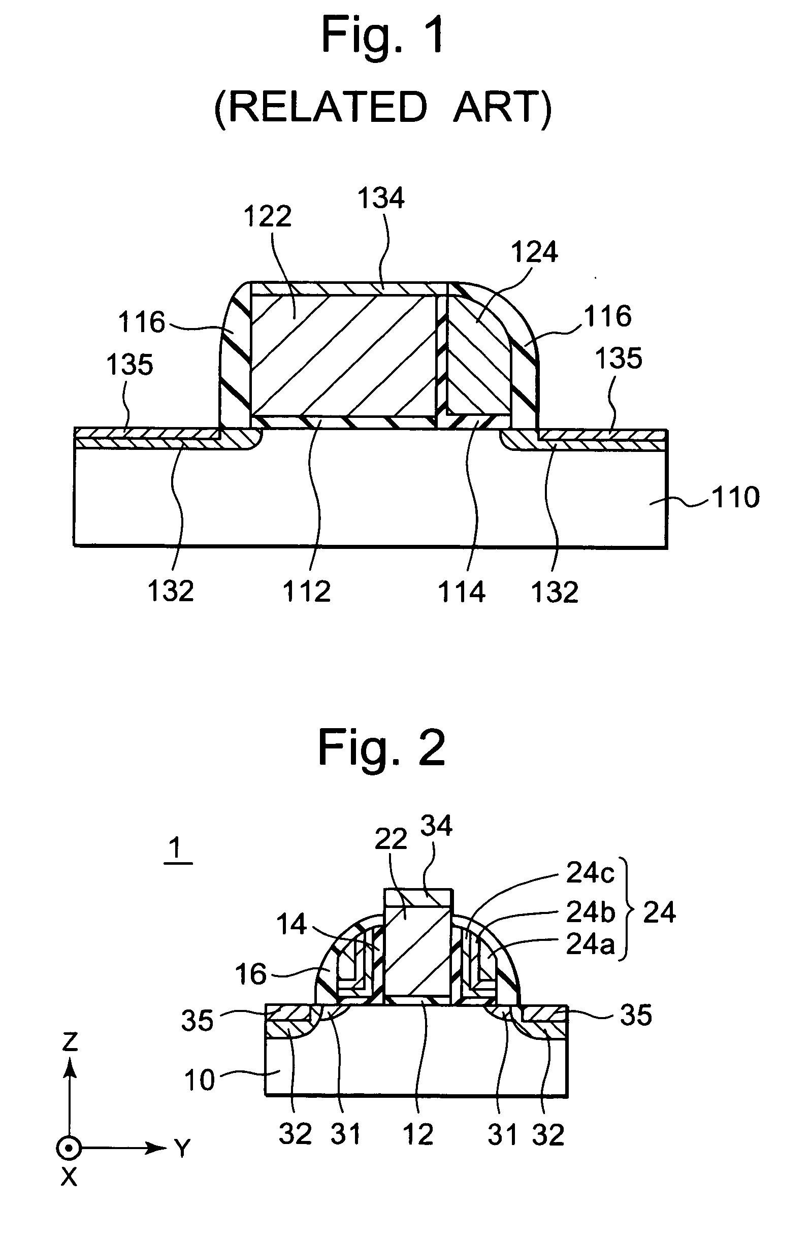
[0008]However, the present inventor has recognized the following point. Namely, the technique disclosed in JP-A-2005-228786 has the following problems. When the gate (word gate) 122 and the
diffusion layer electrodes 132 are silicided (to form the silicide
layers 134 and 135), the memory gate insulating film (charge storage layer) 114 which is the ONO film already has a section of an upper end exposed. When a silicide step is performed while the section of the ONO film is being exposed in this way, a silicide film is formed in the ONO film because nickel components attached onto the
nitride film of the ONO film are easily subjected to a silicide reaction with
silicon in the nitride film. Then, even when the excessive nickel components are removed by
etching, the silicide film is not removed, and remains on the ONO film. As a result, the silicide layer (control gate) 124 and the gate (word gate) 122 may be short-circuited due to the remaining silicide film. A technique for preventing short-circuiting between the ONO film and the control gate is desired.
[0009]Additionally, in this structure, the silicide layer (control gate) 124 which is the silicide film is in direct contact with the memory gate insulating film (charge storage layer) 114 serving as a charge storage region. That is,
nickel silicide which has an extremely
low resistance as compared to polysilicon, comes into direct contact with the ONO film. Thus, it is thought that charges stored in a nitride film of the ONO film are very easily affected by an electric state of the
nickel silicide (for example, variations in
voltage), or a state of an
oxide film (for example, uniformity in film thickness) located on the nickel silicide side of the ONO film. Thus, the electric state and the film thickness state can make the state of charges stored in the nitride film extremely unstable, and make the distribution of charges nonuniform. In particular, nickel components of the nickel silicide may be partly diffused into the
oxide film on the nickel silicide side to degrade the quality of the ONO film. In that case, the charges stored in the nitride film can be prone to penetrate the nickel components. In this way, such occurrence of unstable charges and nonuniform electrolytic distribution at the ONO film, and degradation in quality of the ONO film leads to a
crash of data, which may significantly reduce reliability and stability of a
memory cell. Thus, there is a need for a technique that prevents the
instability of charges and nonuniformity of electrolytic distribution at the ONO film and the degradation in quality of the ONO film, thereby to enhance the reliability and stability of the
memory cell.
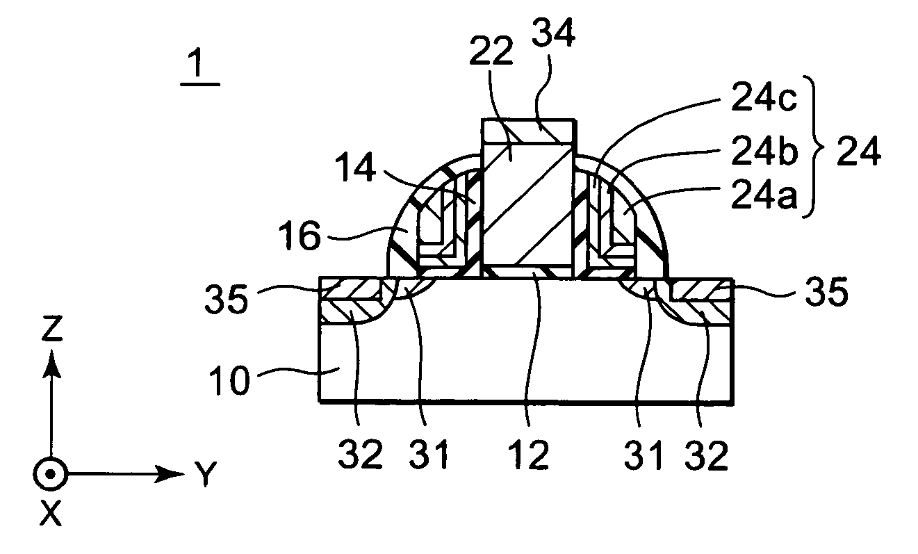
[0012]In this exemplary embodiment, the silicide layer is provided by silicide containing nickel. Therefore, the resistance of the control gate can be made lower. On the other hand, the non-silicide
layers are provided between the silicide layer and the charge storage layer, thereby separating both
layers. Thus, even when a nitride film exposed to the section of the ONO film is partly silicided, the silicide layer is spaced more apart from the word gate, which can prevent short-circuiting. The silicide layer is configured not to be in direct contact with the ONO film by a presence of the non-silicide layers. Thus, the influences of the electric state of the silicide layer, and of the state of an oxide film on the silicide layer side of the ONO film can be reduced to a much smaller level. The nickel components of the silicide layer are prevented from being diffused into the ONO film, so that the charges stored in the nitride film can be prevented from being drawn into the nickel components. Such an arrangement can stabilize more the state of charges stored in the nitride film, make the charge distribution more uniform, and prevent the degradation in quality of the ONO film. As a result, the reliability and stability of the memory
cell can be enhanced.
[0015]The invention can prevent short-circuiting between the word gate and the control gate. The
instability of charges and nonuniformity of electrolytic distribution at the ONO film, the degradation in quality of the ONO film, and the like can be prevented, which can enhance the reliability and stability of the memory
cell.

