

Substrate for magnetic recording medium, magnetic recording medium, and magnetic recording and reproducing apparatus
- Summary
- Abstract
- Description
- Claims
- Application Information
AI Technical Summary
Benefits of technology
Problems solved by technology
Method used
Image

Examples
examples
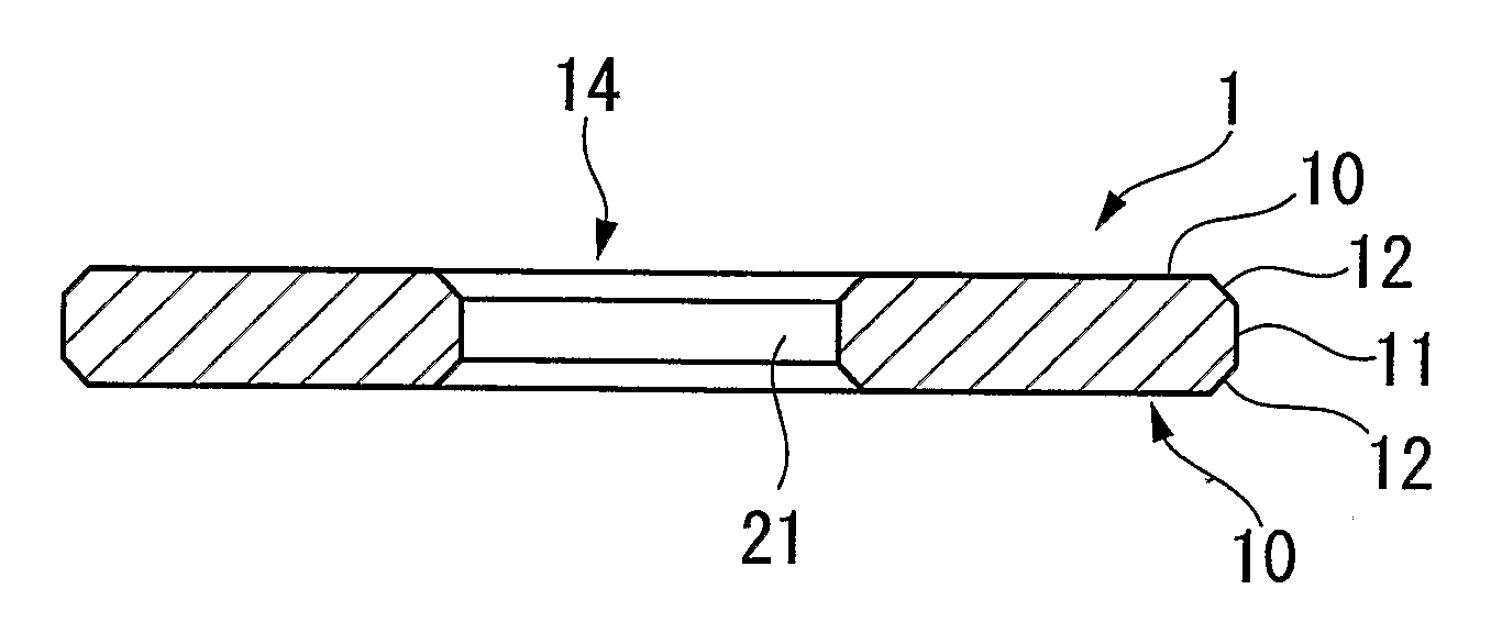
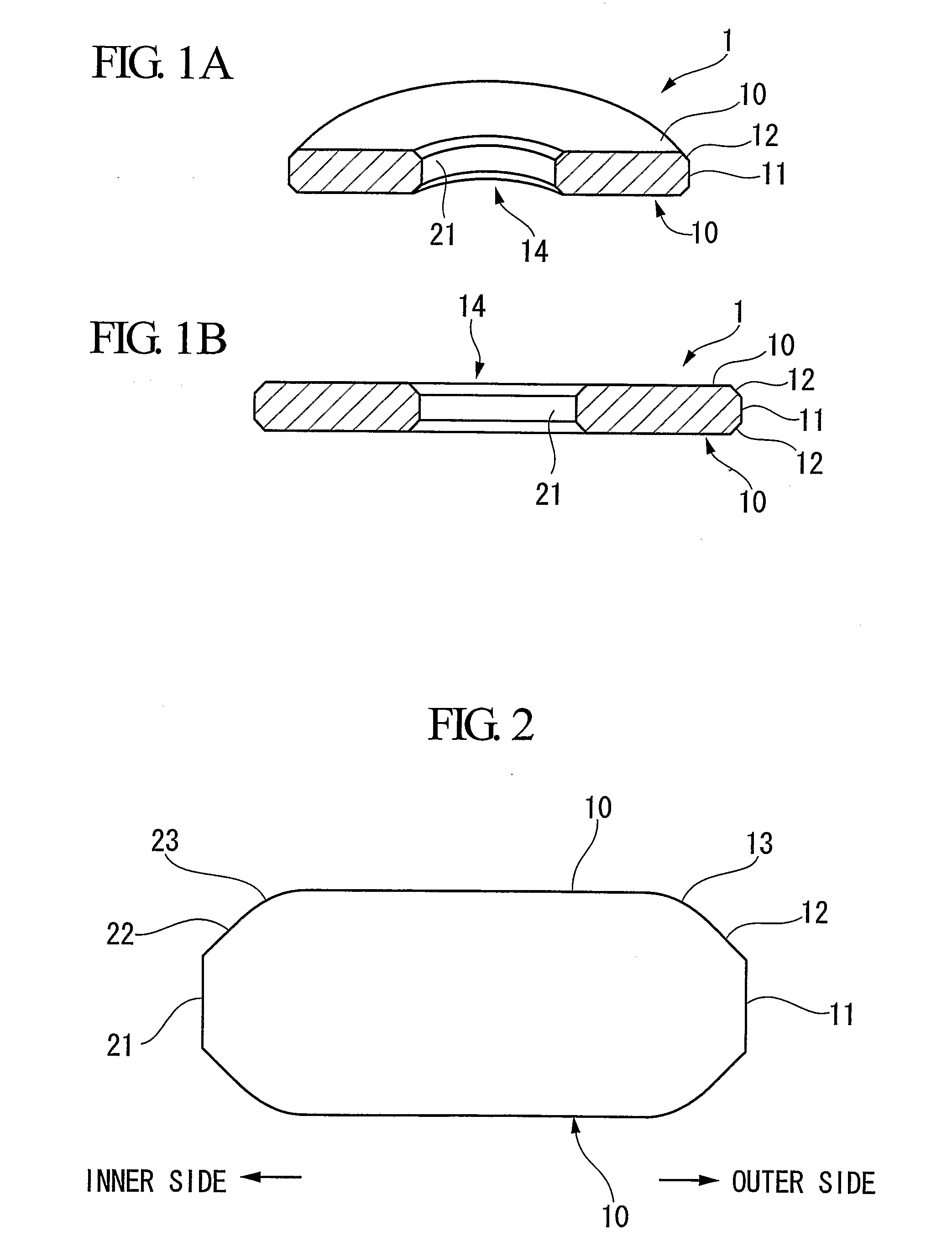
[0087]There were employed glass substrates (amorphous glass substrates and crystallized glass substrates) and silicon substrates (single-crystal silicon substrates for semiconductors). Each substrate was processed to have an outer diameter of 48 mm, an inner diameter of 12 mm, and a thickness of 0.508 mm, and then washed.
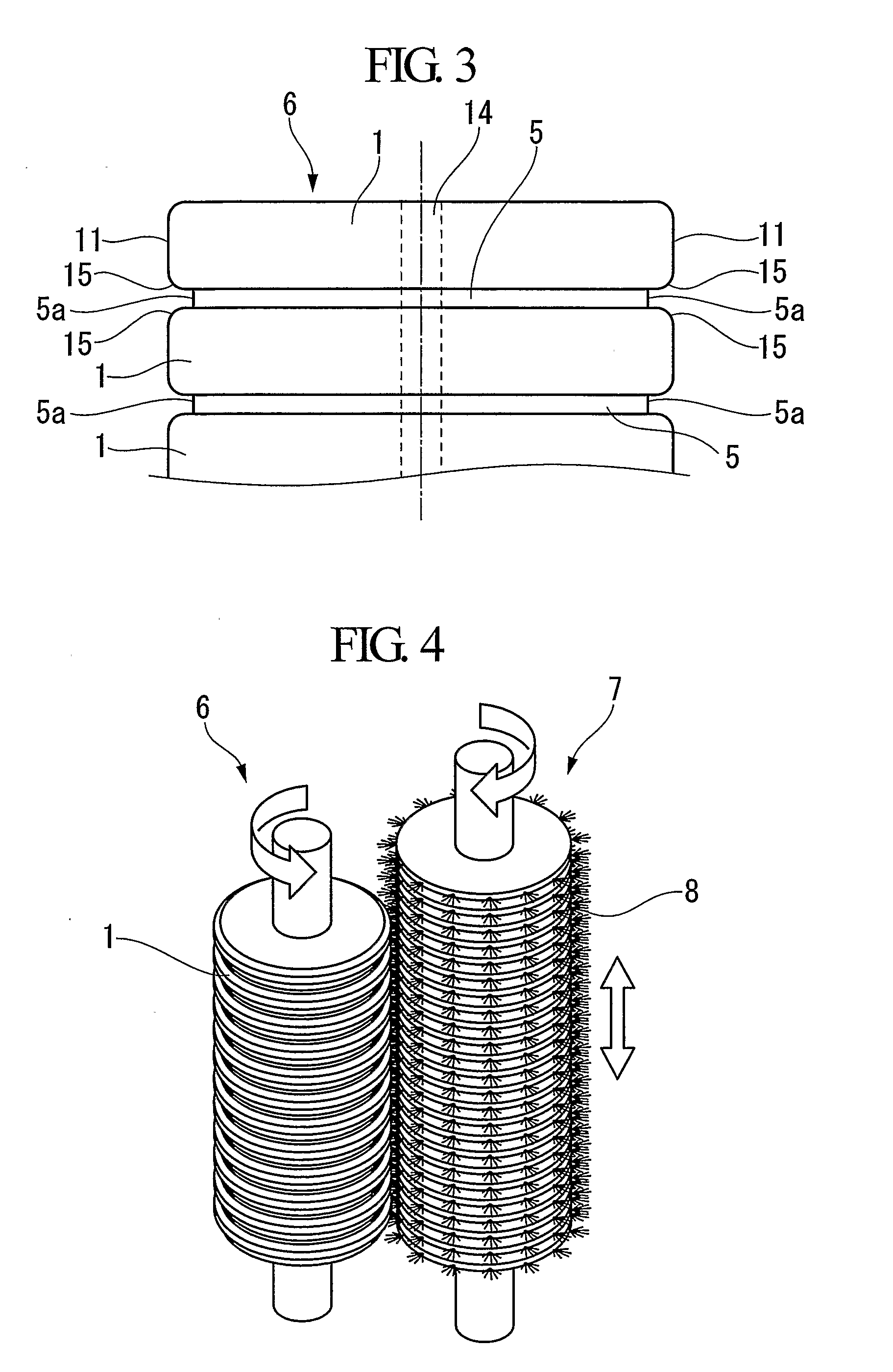
[0088]The substrate samples were formed into a stacked layer body as shown in FIG. 3, and then subjected to brush polishing through the method as shown in FIGS. 4 and 5, to thereby prepare magnetic recording medium substrate products in which the surface roughness (Ra) of the chamfer was regulated to 4.0 Å or more and 100 Å or less as measured by means of an AFM, the surface roughness (Ra) of the outer or inner end surface was regulated to 4.0 Å or more and 100 Å or less, and the R surface curvature was regulated to 0.01 mm or more and 0.07 mm or less.
[0089]Subsequently, each of the thus-prepared substrate products was placed in a film formation chamber of a DC magn...
PUM
| Property | Measurement | Unit |
|---|---|---|
| Length | aaaaa | aaaaa |
| Length | aaaaa | aaaaa |
| Length | aaaaa | aaaaa |
Abstract
Description
Claims
Application Information