Multi-chips package structure and the method thereof

a technology of multi-chips and package structures, applied in the direction of electrical equipment, semiconductor devices, semiconductor/solid-state device details, etc., can solve the problems of more and more complicated chips installed in a very tiny space, solder balls are not easy to be damaged and out of shape, and the previous lead package technology is not compatible with dice with high density of metal pins, etc. cost reduction, cost saving of package materials, cost reduction

Inactive Publication Date: 2009-09-17
CHIPMOS TECH INC
View PDF3 Cites 17 Cited by
  • Summary
  • Abstract
  • Description
  • Claims
  • Application Information

AI Technical Summary

Benefits of technology

[0012]Besides, one another object of the present invention is to provide a multi-chips package method to let the chips sawed from a 12 inches wafer put a chip-placed frame. Therefore, the 8 inches wafer package equipment is still useful and reduce the cost to buy some 12 inches package equipments.
[0013]One other object of the present invention is to provide multi-chips package method to package the chips, which are known as good chips, and the package material can be saved and the cost of the manufacture can be decreased.
[0014]Other project of the present invention is to relocate the chips by the chip-placed areas of the chip-placed frame and the accuracy of the relocation position of the chips is enhanced by the reference position of the chip-placed areas.

Problems solved by technology

Therefore, the previous lead package technology is not compatible for dice with high density of metal pins.
The BGA package method is not only suitable for using in dices with high density of metal pins, but also the solder balls is not easy to be damaged and out of shape.
Because the 3C products, such as cell phone, personal digital assistant (PDA), or MP3 player, are more and more popular in the market, there are more and more complicated chips installed in a very tiny space.
However, when the pads on the active surface of the chips are increased and the interval between the pads is become smaller, the WLP technology will cause the signal overlapped or interrupted problems.
So, when the chip is become further smaller, the previous package methods are not good enough to use.
For example a fan out technology is used, it is able to solve the small interval problem but it may cause the signal overlapped or signal interrupt problems.
Because the chip is very thin, the package structure is also very thin.
Therefore, when the package structure is left from the carrier board, the package structure would be out of shape and it would cause the difficulty to do the sawing process.
After sawing the wafer, because the dice are put on another carrier board, the size of the new carrier board is larger than the original carrier board, the ball mounting process is hard for the solder ball to be installed at the exact location and the reliability of the package structure is reduced.
Besides, in the package procedure, the manufacture equipment will generate more pressure in the dice during the ball mounting process.

Method used


Image

  • Multi-chips package structure and the method thereof
  • Multi-chips package structure and the method thereof
  • Multi-chips package structure and the method thereof

Examples


Embodiment Construction

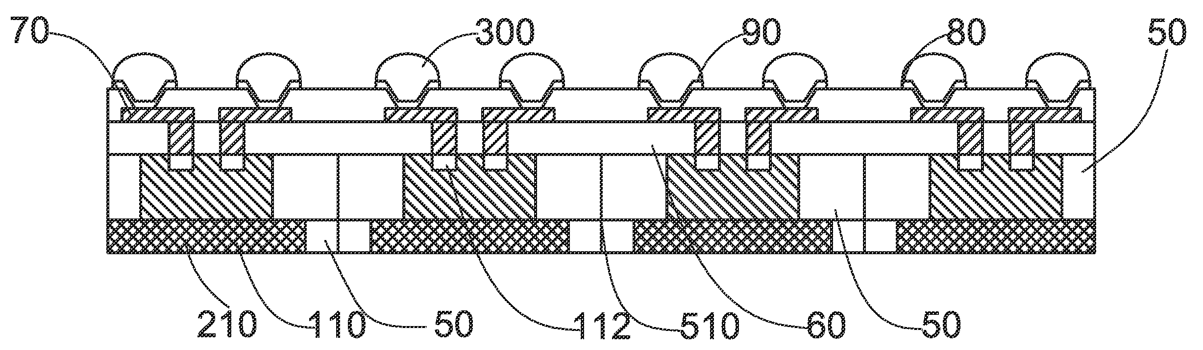
[0036]In the present semiconductor package procedure, the wafer had passed in the front end process needs to do a thinning process first, such as the thickness of the wafer is thinned to 2˜20 mil thick. Then, a sawing process is used to cut the wafer to be several pieces of dice 110 and a means for pick and place is used to put those dice 110 to another carrier board. Obviously, because the interval between the dice on the carrier board is larger than the size of dice, those relocated dice is able to have larger interval. Therefore, the pads on the dice are able to be appropriately distributed.

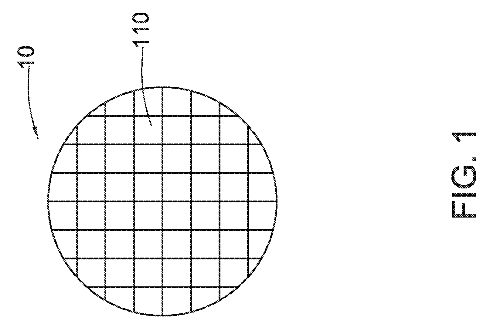
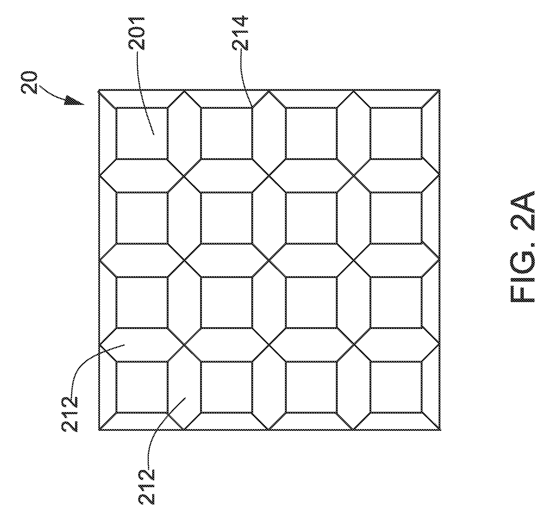
[0037]First, FIG. 1 is a top view showing that there is a plurality of dice 110 in a wafer 10 and each of the dice 110 includes several pads (not shown). FIGS. 2A and 2B are views showing that a chip-placed frame is used to relocate those chips. The chip-placed frame 20 is a reticulated frame and includes a plurality of chip-placed areas 210 with the same size. A plurality of leads 214 are use...


PUM


Abstract

A multi-chips package structure is provided, which includes a chip-placed frame having a plurality of chip-placed areas thereon, and two adjacent chip-placed areas is connected by a plurality of leads; a plurality of chips, each chip has a plurality of pads on an active surface thereon, and is provided on the chip-placed area; a package body is covered around the four sides of the chip-placed frame, and the pads of the chip is to be exposed; one end of a plurality of patterned metal traces is electrically connected to the plurality of pads, another end is extended to cover the surface of the patterned first protection layer; a patterned second protective layer is covered on the patterned metal traces and another end of the patterned metal traces is to be exposed; a plurality of patterned UMB layer is formed on the extended surface of the patterned metal traces; and a plurality of conductive elements is formed on the patterned UMB layer and is electrically connected to one end of the exposed portion of the patterned metal traces.

Description

BACKGROUND OF THE INVENTION[0001]1. Field of the Invention[0002]The present invention is relates to a multi-chips package method, and more particularly is related to a package method by utilizing a chip-placed frame to relocate the chips.[0003]2. Description of the Prior Art[0004]The semiconductor technology is well developed and grown up very fast. Because the microlized semiconductor dice are required to include more functions, the semiconductor dice are necessary to have more input / output (I / O) pads. The density of the metal pins is higher day after day. Therefore, the previous lead package technology is not compatible for dice with high density of metal pins. A Ball Grid Array (BGA) package method is used for dices with high density of metal pins. The BGA package method is not only suitable for using in dices with high density of metal pins, but also the solder balls is not easy to be damaged and out of shape.[0005]Because the 3C products, such as cell phone, personal digital as...

Claims


Application Information

Patent Timeline
Patent Type & Authority Applications(United States)
IPC IPC(8): H01L23/495H01L21/56
CPCH01L21/561H01L2224/12105H01L23/49541H01L24/19H01L24/96H01L24/97H01L25/50H01L2224/04105H01L2224/20H01L2224/97H01L2924/01029H01L2924/01082H01L2924/01094H01L23/3114H01L2224/0401H01L2924/01005H01L2924/01033H01L2224/32245H01L2224/73267H01L2224/92244H01L2224/8203H01L2224/82H01L2924/181H01L2924/00
Inventor SHEN, GENG-SHIN
Owner CHIPMOS TECH INC
Why Eureka
Try Eureka