System for handling semiconductor module

a technology for semiconductor modules and systems, applied in the field of systems for handling semiconductor modules, can solve the problems of difficult simultaneous and rapid handling of a relatively large amount of semiconductor modules held in a multi-layered structure in a relatively small space, time-consuming process for testing semiconductor modules, etc., and achieves the effect of efficient configuration, fast and correctly handling, and preventing or reducing interferen

Active Publication Date: 2009-09-24
SAMSUNG ELECTRONICS CO LTD
View PDF10 Cites 5 Cited by
  • Summary
  • Abstract
  • Description
  • Claims
  • Application Information

AI Technical Summary

Benefits of technology

[0010]Example embodiments provide a system for handling a semiconductor module, which is efficiently configured by preventing or reducing interferences between sensors and installation cables such that an operation of handling a semiconductor module may be automated and a relatively large number of semiconductor modules, which may be held in a multi-layered structure in a relatively small space, may be quickly and correctly handled.

Problems solved by technology

Manually testing the semiconductor modules may be a time consuming process, and various problems frequently occur due to operator's mistakes during handling operations when the semiconductor modules are moved, inserted, and extracted.
However, developing and using robots for this purpose may be difficult because of the shape difference between a socket and a tray.
For example, simultaneously and quickly handling a relatively large amount of semiconductor modules that are held in a multi-layered structure in a relatively small space may be difficult.
In addition, handling the semiconductor modules may be difficult because an interval between a socket and a tray may be relatively small due to use of various sensors and many cables.

Method used


Image

  • System for handling semiconductor module
  • System for handling semiconductor module
  • System for handling semiconductor module

Examples


Embodiment Construction

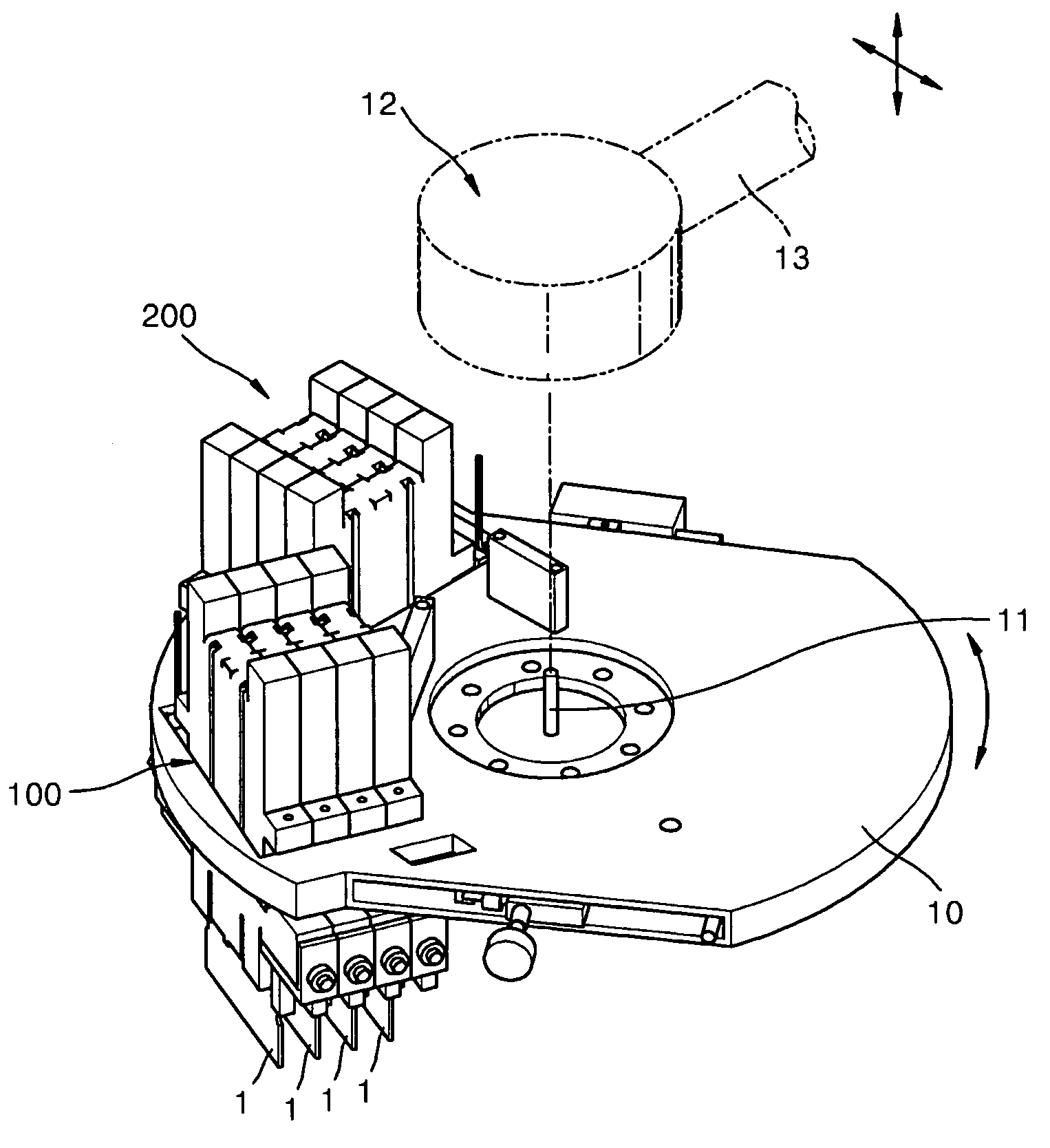
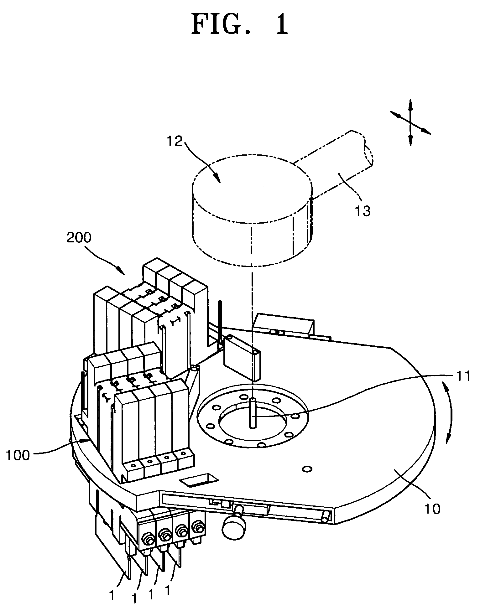
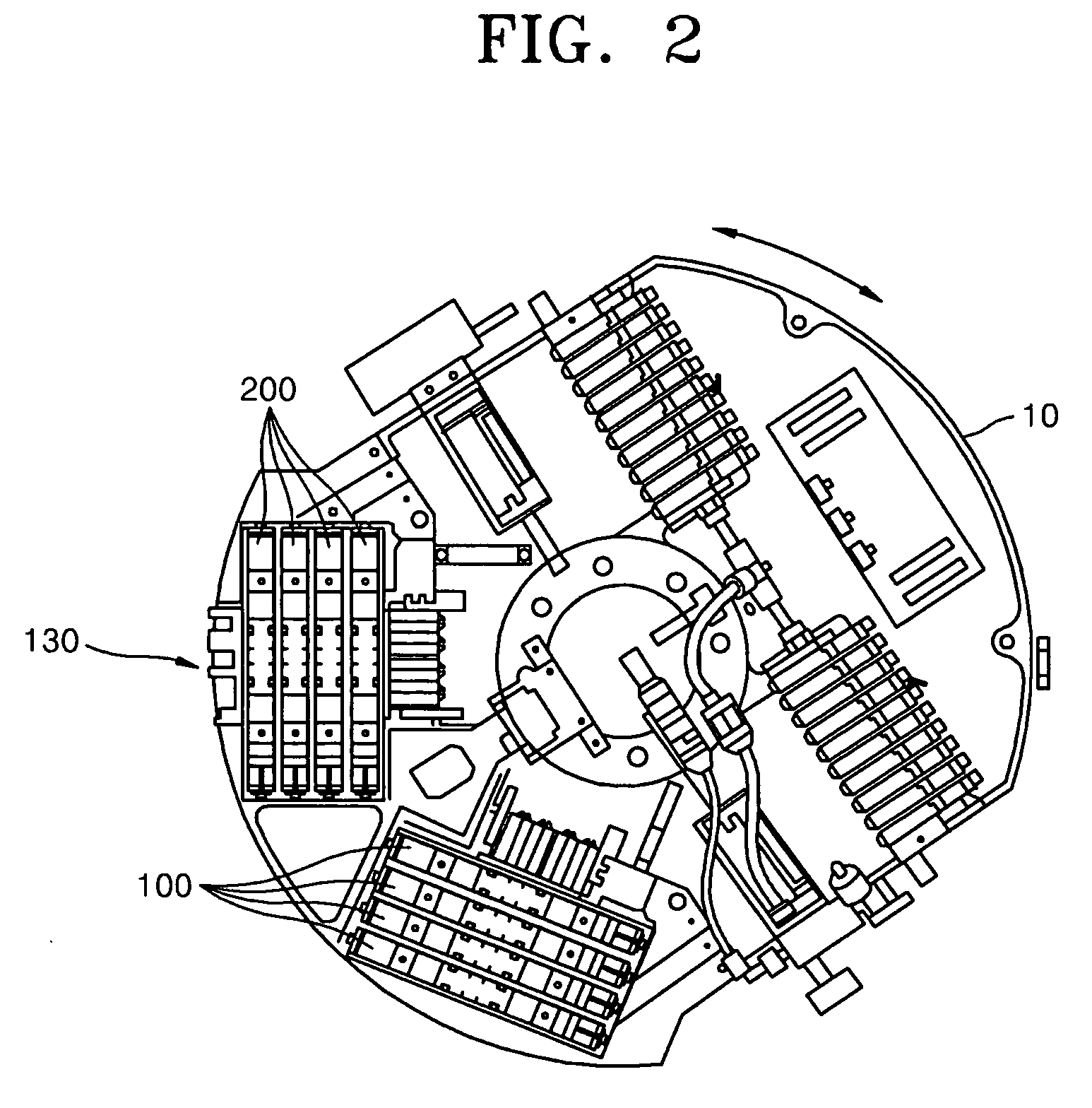
[0028]Example embodiments will now be described more fully with reference to the accompanying drawings, in which example embodiments are shown. The invention may, however, be embodied in different forms and should not be construed as limited to the embodiments set forth herein. Rather, these embodiments are provided so that this disclosure will be thorough and complete, and will fully convey the scope of the invention to those skilled in the art. In the drawings, the sizes of components may be exaggerated for clarity.

[0029]It will be understood that when an element or layer is referred to as being “on”, “connected to”, or “coupled to” another element or layer, it can be directly on, connected to, or coupled to the other element or layer or intervening elements or layers that may be present. In contrast, when an element is referred to as being “directly on”, “directly connected to”, or “directly coupled to” another element or layer, there are no intervening elements or layers present...


PUM

PropertyMeasurementUnit
hydraulic pressureaaaaaaaaaa
distanceaaaaaaaaaa
shapeaaaaaaaaaa

Abstract

Provided is a system for handling a semiconductor module, the system may include a rotor, a rotational driving device, at least one insertion portion, and at least one extraction portion. The rotor may be configured to rotate clockwise and counterclockwise around a rotation axis. The rotational driving device may be configured to rotate the rotor. The at least one insertion portion may be connected to the rotor and may be configured to insert a semiconductor module into a socket. The at least one extraction portion may be connected to the rotor and may be configured to extract the semiconductor module from the socket.

Description

PRIORITY STATEMENT[0001]This application claims priority under 35 U.S.C. §119 to Korean Patent Application No. 10-2008-0024890, filed on Mar. 18, 2008, in the Korean Intellectual Property Office (KIPO), the entire contents of which are herein incorporated by reference.BACKGROUND[0002]1. Field[0003]Example embodiments relate to a system for handling a semiconductor module, and more particularly, to a system for handling a semiconductor module that allows operation of testing the semiconductor module to be performed.[0004]2. Description of the Related Art[0005]A semiconductor chip may be formed on a wafer using a semiconductor manufacture process. The semiconductor chip may be separated from the wafer in a separate process, and the manufacture of a semiconductor device may be completed using a packaging processes.[0006]The completed semiconductor device may be combined with a circuit board having a circuit pattern in order to make a semiconductor module. Prior to finalizing the semico...

Claims


Application Information

Patent Timeline
Patent Type & Authority Applications(United States)
IPC IPC(8): B65G49/00B65G47/00B65G29/00
CPCG01R31/2893G01R31/26H01L22/00
Inventor PARK, CHUL-JUNSHIN, YONG-SOOHWANG, JAE-WOONGKIM, JIN-GI
Owner SAMSUNG ELECTRONICS CO LTD
Why Eureka
Try Eureka