
Method of forming metal wiring

Inactive Publication Date: 2009-09-24
SAMSUNG ELECTRONICS CO LTD
View PDF1 Cites 32 Cited by
  • Summary
  • Abstract
  • Description
  • Claims
  • Application Information

AI Technical Summary

Benefits of technology

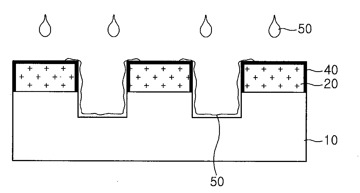
[0010]Aspects of the present invention provide a method of forming buried metal wiring, in which a waste of metal material can be prevented, and thus manufacturing costs can be reduced.
[0011]Aspects of the present invention also provide a method of forming buried metal wiring, in which no metal thin film is formed on a photosensitive film pattern when a seed layer is formed, thereby preventing a waste of metal material.

Problems solved by technology

If such a large step height is created in a lower substrate, it undermines liquid crystal filling.
Accordingly, liquid crystal molecules are not uniformly aligned, and a uniform transmittance cannot be obtained, thereby deteriorating display quality of the LCD.
The discarded metal thin film is essentially wasted, which in turn increases manufacturing costs.
Therefore, it is difficult to remove the metal thin film in the lift-off process.

Method used


Image

  • Method of forming metal wiring
  • Method of forming metal wiring
  • Method of forming metal wiring

Examples


Embodiment Construction

[0027]Advantages and features of the present invention and methods of accomplishing the same may be understood more readily by reference to the following detailed description of exemplary embodiments and the accompanying drawings. The present invention, including numerical values of various variables, may, however, be embodied in many different forms and take on many different values, and should not be construed as being limited to the embodiments set forth herein. Rather, these embodiments are provided so that this disclosure will be thorough and complete and will fully convey the concept of the invention to those skilled in the art, and the present invention will only be defined by the appended claims. In the drawings, the thickness of the layers and regions are exaggerated for clarity. Like reference numerals refer to like elements throughout the specification. When an element such as a layer, film, region, or substrate is referred to as being “on” another element, it can be dire...


PUM

PropertyMeasurementUnit
Levelaaaaaaaaaa
Photosensitivityaaaaaaaaaa

Abstract

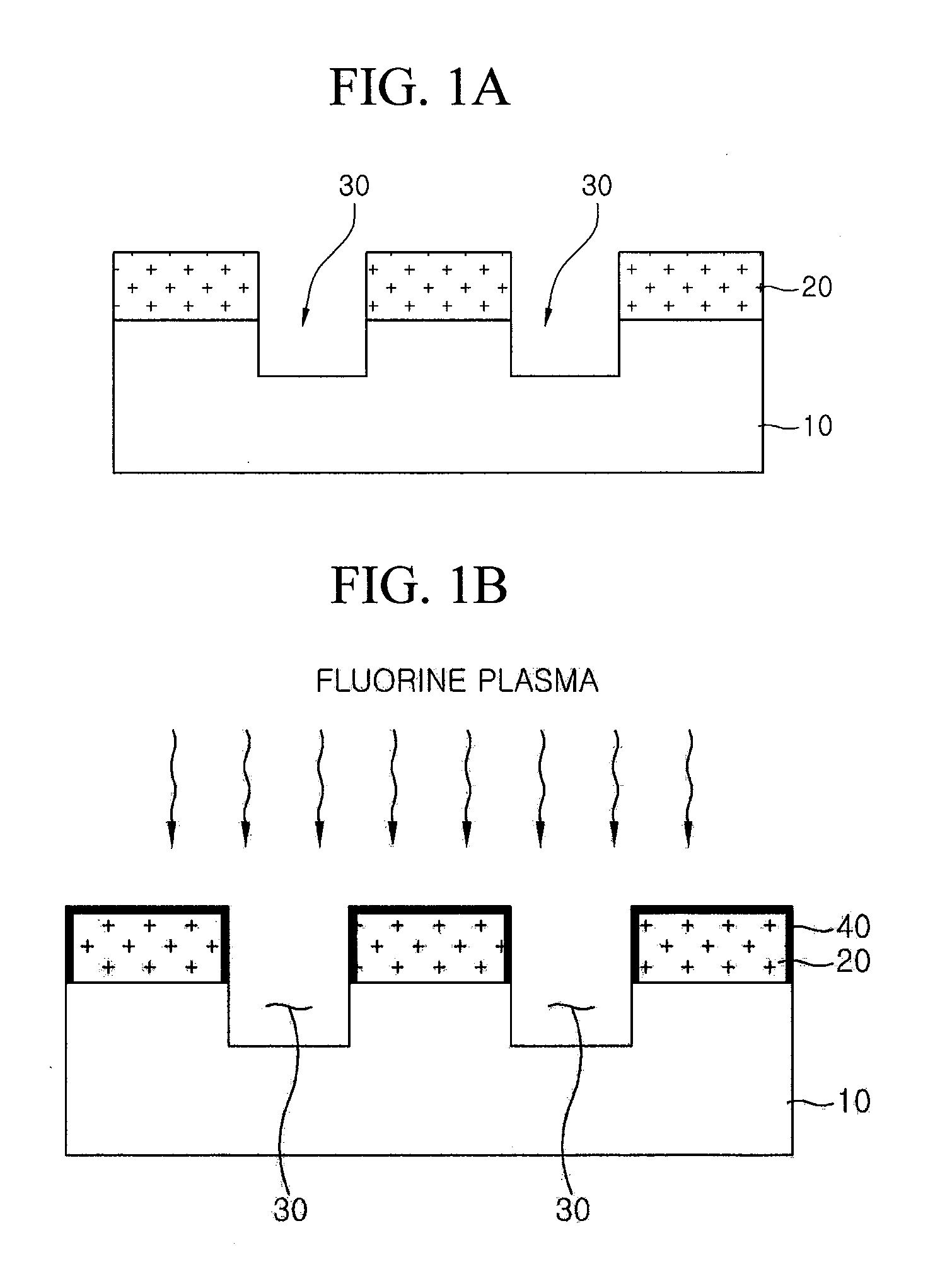
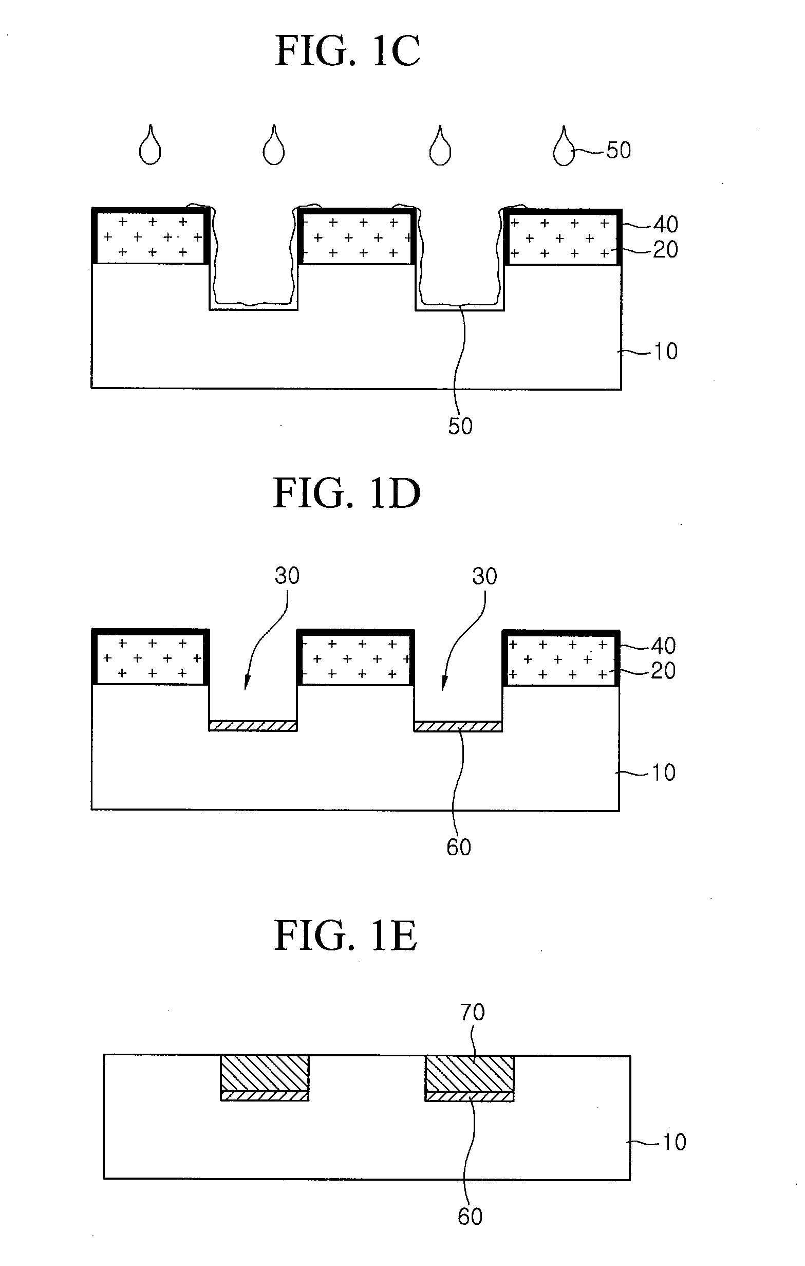
Provided is a method of forming metal wiring. The method includes forming a photosensitive film pattern on a substrate, hydrophobicizing at least part of the photosensitive film pattern, coating metal ink on the substrate having the photosensitive film pattern, forming a seed layer, and forming a metal layer. Alternatively, a trench is formed by using the photosensitive film pattern as a mask, and metal aerosol is sprayed to form the seed layer and then the metal layer. In this method, there is no need to form a metal thin film on the photosensitive film pattern when the seed layer is formed. As a result, less metal is wasted, which, in turn, significantly reduces manufacturing costs.

Description

[0001]This application claims priority from Korean Patent Application No. 10-2008-0025537 filed on Mar. 19, 2008 and 10-2008-0032382 filed on Apr. 7, 2008 in the Korean Intellectual Property Office, the disclosure of which is incorporated herein by reference in its entirety.BACKGROUND OF THE INVENTION[0002]1. Field of the Invention[0003]The present invention relates to a method of forming metal wiring, and more particularly, to a method of forming buried metal wiring.[0004]2. Description of the Related Art[0005]Liquid crystal displays (LCDs) are one of the most widely used flat panel displays (FPDs). An LCD includes a lower substrate on which gate lines, data lines, pixel electrodes, TFTs and the like are formed, an upper substrate on which common electrodes are formed, and a liquid crystal layer which is interposed between the lower and upper substrates. The LCD applies voltages to the pixel electrodes and the common electrodes and thus generates an electric field in the liquid cry...

Claims


Application Information

Patent Timeline
IPC IPC(8): H01L33/00G03F7/26H01L21/02C25D7/06H01L23/52
CPCC25D1/04H01L27/1218G02F2001/136295H01L21/288H01L21/76843H01L21/76871H01L21/76879H05K3/002H05K3/107H05K3/1258H05K3/246H05K2201/0108H05K2201/0347H05K2203/0568H05K2203/095H05K2203/1173H01L27/124H01L27/1292C25D5/022G02F1/136295
Inventor KIM, JANG-SUBKANG, YOON-HOBAE, YANG-HOYUN, PIL-SANGJEONG, CHANG-OHLIM, SOON-KWONPARK, HONG-SICKLONG, NING HONGKIM, DO-HYUNJUNG, SEUNG-JAE
Owner SAMSUNG ELECTRONICS CO LTD
Learn More