Electronic component mounting board, method for manufacturing the same and electronic circuit unit

a technology for mounting boards and components, applied in the direction of dielectric characteristics, fixed connections, semiconductor/solid-state device details, etc., can solve the problems of high cost, difficult to make the pitch narrow, and high cost of anisotropic conductive elastomers, etc., to achieve excellent conductivity, low contact resistance and inductance, and sufficient contact pressure

Inactive Publication Date: 2009-10-01
THE FUJIKURA CABLE WORKS LTD
View PDF6 Cites 16 Cited by
  • Summary
  • Abstract
  • Description
  • Claims
  • Application Information

AI Technical Summary

Benefits of technology

[0010]The present invention has been achieved in view of the above circumstances, and has an object to provide an electronic component mounting board that is capable of securing a sufficient contac

Problems solved by technology

Moreover, it is difficult to make the pitch narrow.
Furthermore, high costs are required because an anisotropic conductive elastomer sheet itself is expensive.
However, this will decrease the deformability of the conductive elastomer pillars 103.
That is, the conductive elastomer pillars 103 become highly elastic rigid bodies, for which it is difficult to have a displacement amount su

Method used


Image

  • Electronic component mounting board, method for manufacturing the same and electronic circuit unit
  • Electronic component mounting board, method for manufacturing the same and electronic circuit unit
  • Electronic component mounting board, method for manufacturing the same and electronic circuit unit

Examples


first embodiment

[0069]Hereunder is a detailed description of the present invention with reference to the drawings. However, the present invention is not limited to this. Various modifications can be made as long as they do not depart from the spirit or scope of the present invention.

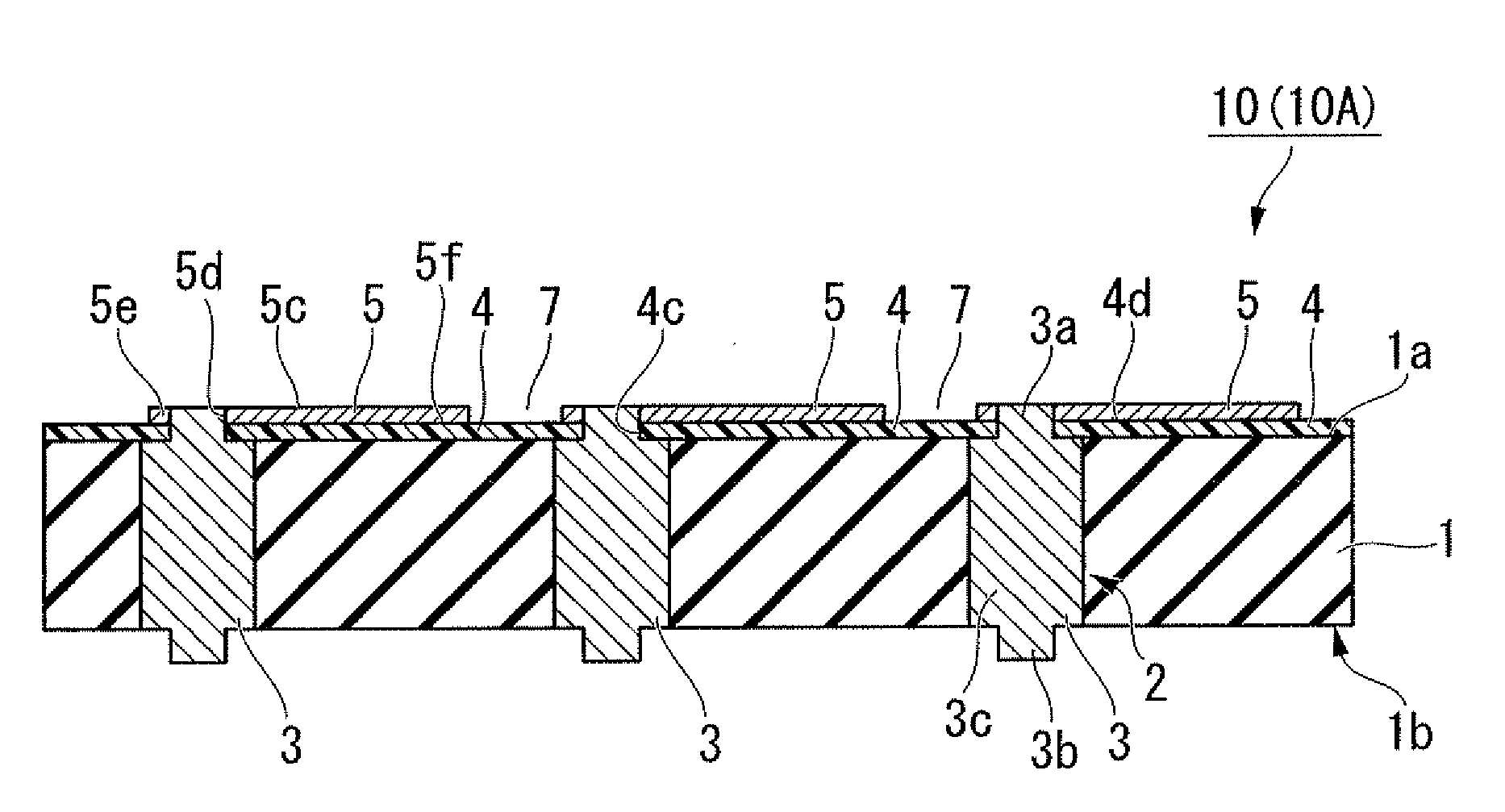
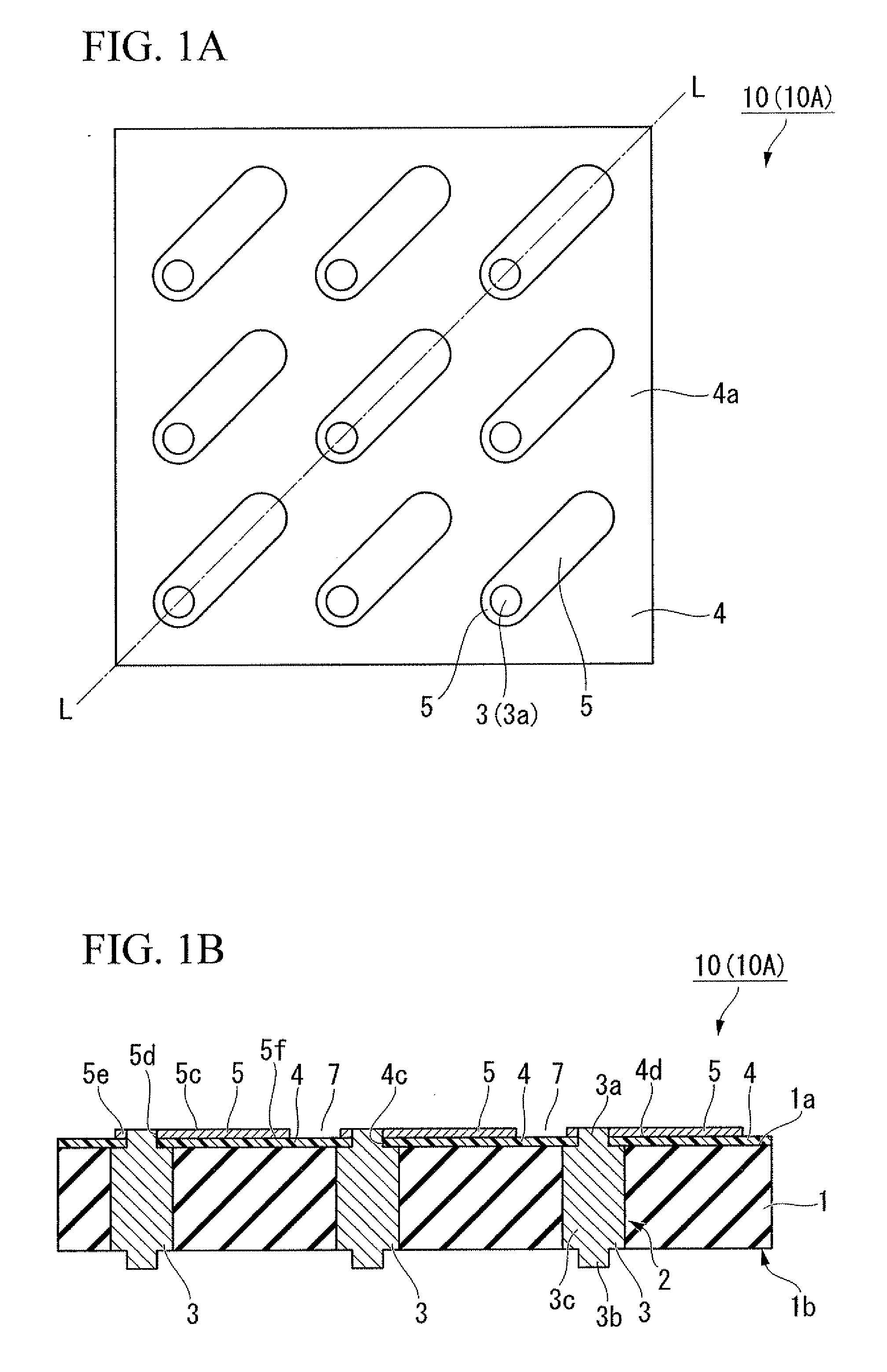
[0070]FIGS. 1A, 1B schematically show a first embodiment of an electronic component mounting board 10 (10A) of the present invention. FIG. 1A is a top view thereof. FIG. 1B is a cross-sectional view of FIG. 1A taken along the line L-L.

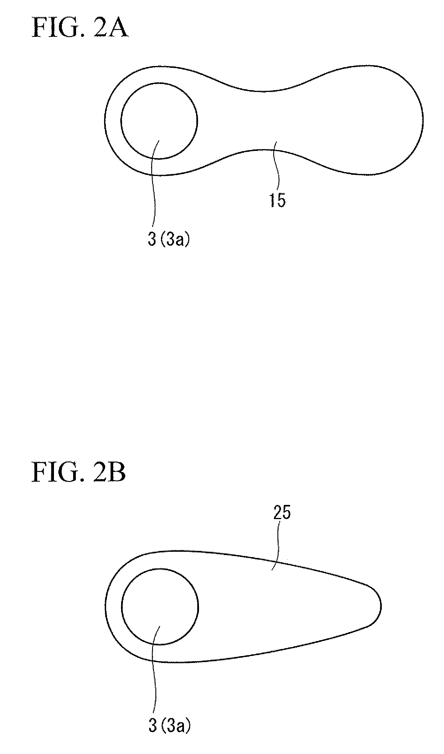
[0071]The electronic component mounting board 10A of the present invention roughly includes: a substrate base 1 made of a flat-plate-like elastic body, the substrate base 1 having a plurality of through-holes 2 in a manner spaced a predetermined distance apart from each other; conductive members 3, each of which has a main unit portion 3c filled in the through-hole 2, the main unit portion 3c having a first protrusion portion 3a and a second protrusion portion 3b respectively on a first en...

second embodiment

[0097]FIGS. 7A, 7B schematically show an electronic component mounting board 10 (10B) according to a second embodiment of the present invention. Like constituent parts to those of the first embodiment may be designated with like reference numerals and may not be repetitiously explained. FIG. 7A is a top view thereof. FIG. 7B is a cross-sectional view of FIG. 7A taken along the line L-L. The difference between the present embodiment and the first embodiment lies in that slits 9 are arranged on the substrate 4, each along the shape of the second end 5f side of the electrode 5.

[0098]The slit 9 may be arranged so as to surround at least an outer circumference on a second end 5f side of the electrode 5. With the slits 9, the stroke amount of the electrode 5 is increased, to thereby make it possible to further absorb irregularities in height of the solder bumps α when the electronic component 60 is mounted, similarly to the case of the first embodiment. Therefore, it is possible to adjust...

third modification

[0100]FIGS. 8A, 8B schematically show an electronic component mounting board 10 (10C) according to a third embodiment of the present invention. Like constituent parts to those of the second embodiment may be designated with like reference numerals and may not be repetitiously explained. FIG. 8A is a top view thereof. FIG. 8B is a cross-sectional view of FIG. 8A taken along the line L-L. The difference between the present embodiment and the second embodiment lies in that structures 6 (6a, 6b) are arranged on both sides 1a, 1b of the substrate base 1.

[0101]With the substrates 4 (4a, 4b) on which electrodes 5 (5a, 5b) are arranged, that is, structures 6 (6a, 6b) being provided on both sides 1a, 1b of the substrate base 1 as in the present embodiment, it is possible to further absorb irregularities in height on both sides of the substrate base 1 when an electronic component or the like is mounted. Therefore, it is possible to mount the electronic component 60 and circuit board 70 with i...


PUM

PropertyMeasurementUnit
Shapeaaaaaaaaaa

Abstract

An electronic component mounting board, including: a substrate base made of a flat-plate-like elastic body, the substrate base having a plurality of through-holes in a manner spaced a predetermined distance apart from each other; conductive members, each of which has a main unit portion filled in the through-hole, the main unit portion having a first protrusion portion and a second protrusion portion respectively on a first end and a second end thereof, with the first protrusion portion arranged so as to protrude from a first surface of the substrate base and the second protrusion portion arranged so as to protrude from a second surface of the substrate base; a flexible substrate that is arranged on the first surface of the substrate base and that has first opening portions for penetration of the first protrusion portions; and a plurality of oval electrodes arranged on the substrate, each of which has a second opening portion for penetration of the first protrusion portion, in which the electrodes are arranged in a manner spaced apart from each other, and each of the second opening portions is formed on a first end side of each of the electrodes.

Description

[0001]Priority is claimed on Japanese Patent Application No. 2008-079587, filed on Mar. 26, 2008, and Japanese Patent Application No. 2008-095019, filed on Apr. 1, 2008, the contents of which are incorporated herein by reference.BACKGROUND OF THE INVENTION[0002]1. Field of the Invention[0003]The present invention relates to an electronic component mounting board. More particularly, the present invention relates to an electronic component mounting board that is capable of securing a sufficient contact pressure irrespective of irregularities in height of electronic components and is also capable of lowering conduction resistance and inductance, relates to a method for manufacturing the same and relates to an electronic circuit unit provided with the electronic component mounting board.[0004]2. Description of Related Art[0005]As conventional methods of mounting an electronic component on a circuit board with electrodes with different heights and on the like, there are disclosed: a meth...

Claims


Application Information

Patent Timeline
IPC IPC(8): H05K1/02H05K3/00
CPCH01R13/24Y10T29/49124H05K1/036H05K3/326H05K3/4046H05K2201/0133H05K2201/09081H05K2201/0949H05K2201/09845H05K2201/10378H05K2201/10416H05K2201/10734H05K2203/063H01R12/52H01L2224/16225H05K1/0313H01L23/12H05K1/02H05K3/34
Inventor ISHII, YUUNAOE, KUNIHIRO
Owner THE FUJIKURA CABLE WORKS LTD
Why Eureka
Try Eureka