

Variable resistor array and amplifier circuit
a resistor array and variable resistor technology, applied in the field of variable resistor arrays, can solve the problem that the above-mentioned mos transistors cannot be easily manufactured
- Summary
- Abstract
- Description
- Claims
- Application Information
AI Technical Summary
Benefits of technology
Problems solved by technology
Method used
Image

Examples
first embodiment
Configuration
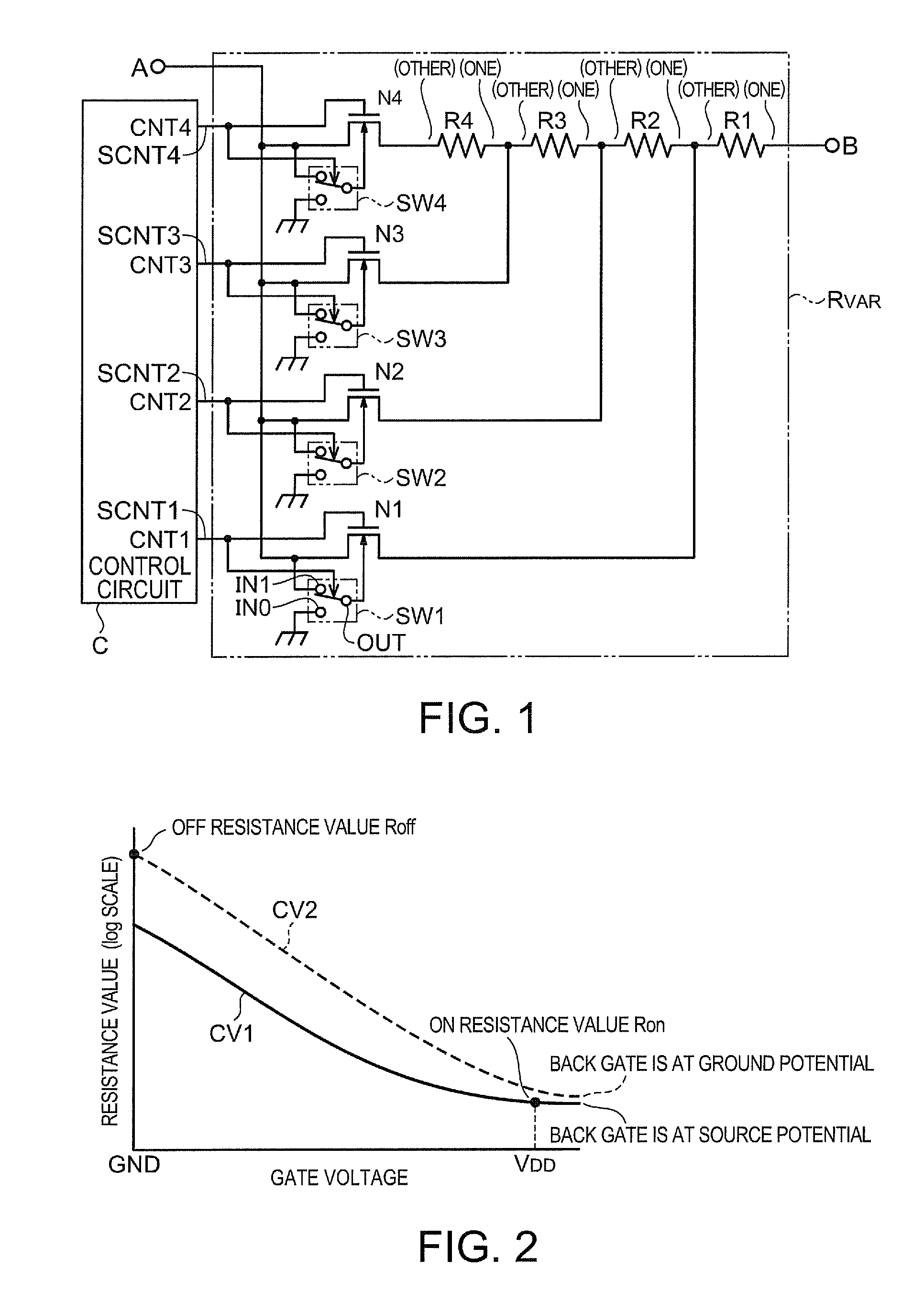
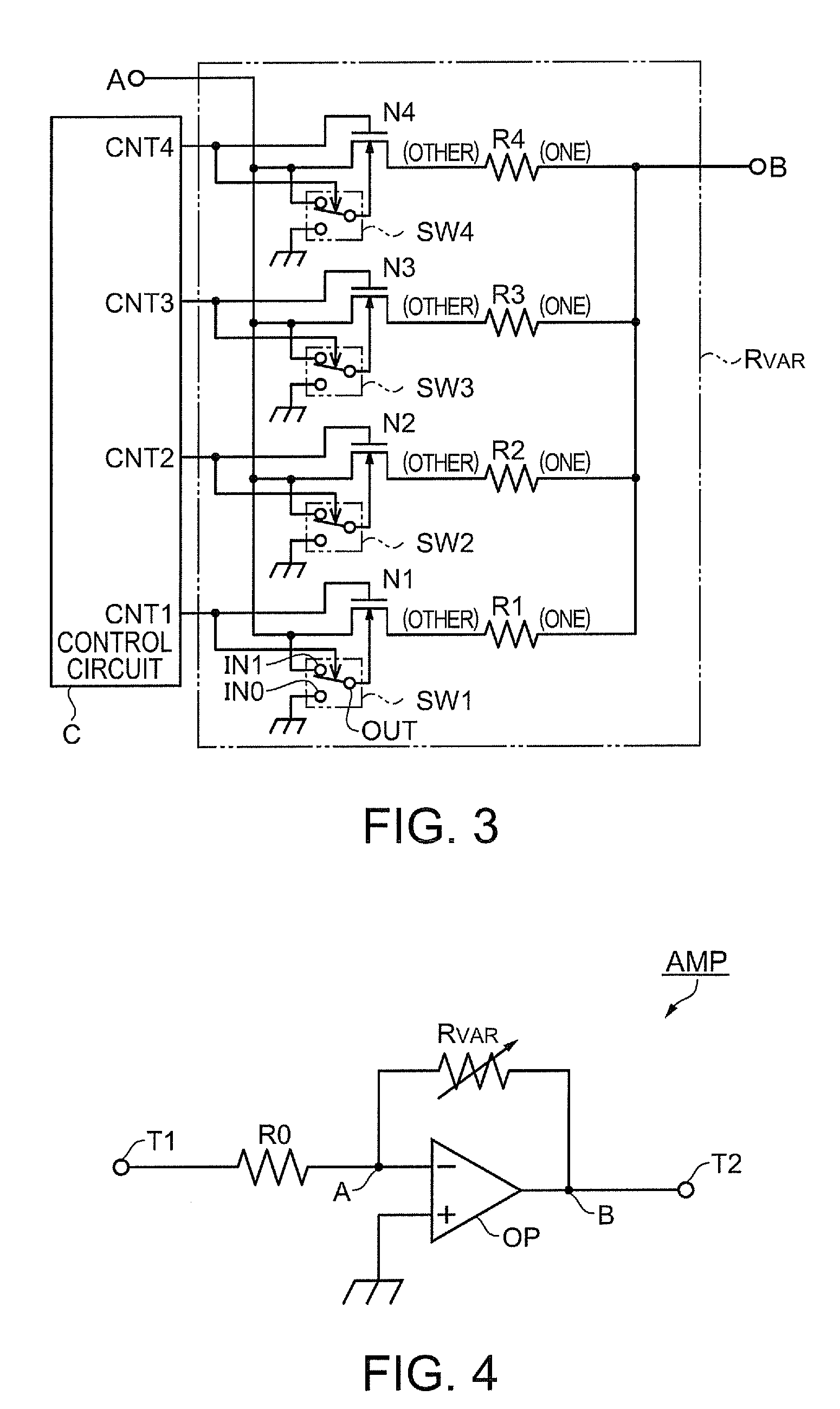
[0026]As shown in FIG. 4, the amplifier circuit AMP includes an amplifier OP, a resistor R0, and a variable resistor (hereinafter referred to as a “variable resistor array”) RVAR in order for amplifying a signal, which is input to an input terminal T1, and then outputting the amplified signal from an output terminal T2 in a basically similar manner to the related art.
[0027]The amplifier OP is, for example, an operational amplifier, having a non-inverted input terminal (+) connected to a potential higher than the ground potential, the resistor R0 is connected between an inverted input terminal (−) of the operational amplifier and the input terminal T1, the variable resistor array RVAR is connected between the inverted input terminal (−) and an output terminal of the operational amplifier, and the output terminal of the operational amplifier is connected to the output terminal T2.
[0028]Hereinafter, the position of the inverted input terminal (−) of the amplifier OP is ref...
second embodiment
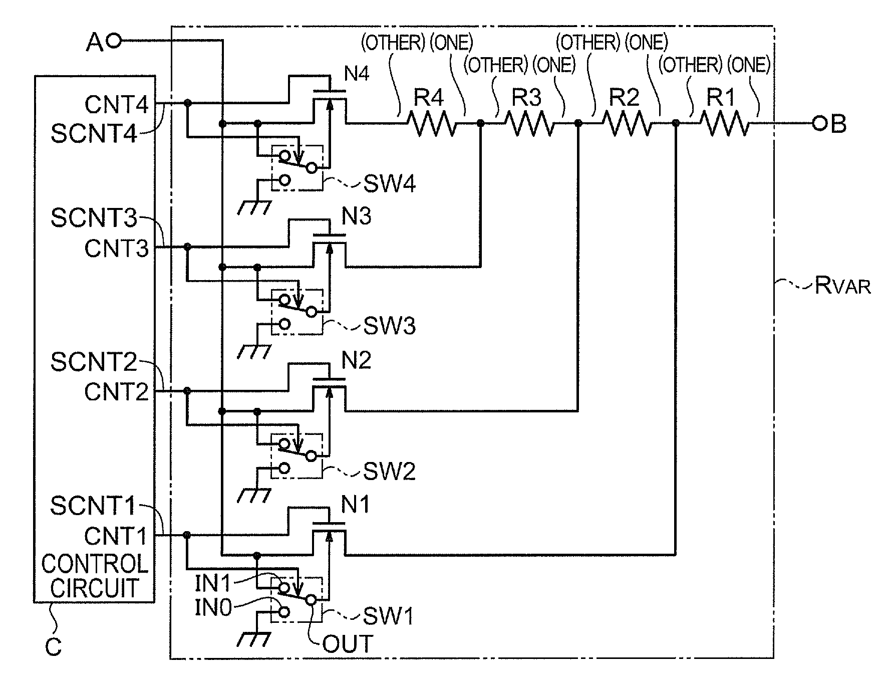
[0053]FIG. 3 shows a configuration of a variable resistor array of the second embodiment. The variable resistor array RVAR of the second embodiment is disposed between the point A and the point B in the amplifier circuit AMP shown in FIG. 4 similarly to the variable resistor array RVAR of the first embodiment, and includes four resistors R1 through R4, four switches SW1 through SW4, and four transistors N1 through N4 as shown in FIG. 3.
[0054]In the variable resistor array RVAR of the second embodiment, in contrast to the variable resistor array RVAR of the first embodiment, the four resistors R1 through R4 are connected in parallel to each other. One ends of the four resistors R1 through R4 are connected to the point B, and the other ends thereof are connected to the drains of the transistors N1 through N4, respectively. The relation of connections between the gates, the back gates, and the sources of the transistors N1 through N4, and the input terminals IN0, the input terminals IN...
modified example
[0061]The same advantages as described above can be obtained by configuring the variable resistor array of a modified example of the first and second embodiments with n (n is an integer equal to or greater than 2) groups (each composed of the resistor, the switch, and the transistor) instead of four groups described above in the first and second embodiments.
[0062]The variable resistor array of the modified example uses PMOS transistors instead of the NMOS transistors described above, and has the input terminals IN0 of the switches SW1 through SW4 connected to the “power supply potential VDD,” thereby also providing substantially the same advantages as described above.
PUM
 Abstract
Description
Claims
Application Information