
Molecular quantum interference apparatus and applications of same

a quantum interference and molecular technology, applied in the field of molecular electronics, can solve the problems of slow switching speed and unaddressed need in the art, and achieve the effect of improving the stability and stability of the devi

Inactive Publication Date: 2009-10-08
NORTHWESTERN UNIV
View PDF0 Cites 6 Cited by
  • Summary
  • Abstract
  • Description
  • Claims
  • Application Information

AI Technical Summary

Benefits of technology

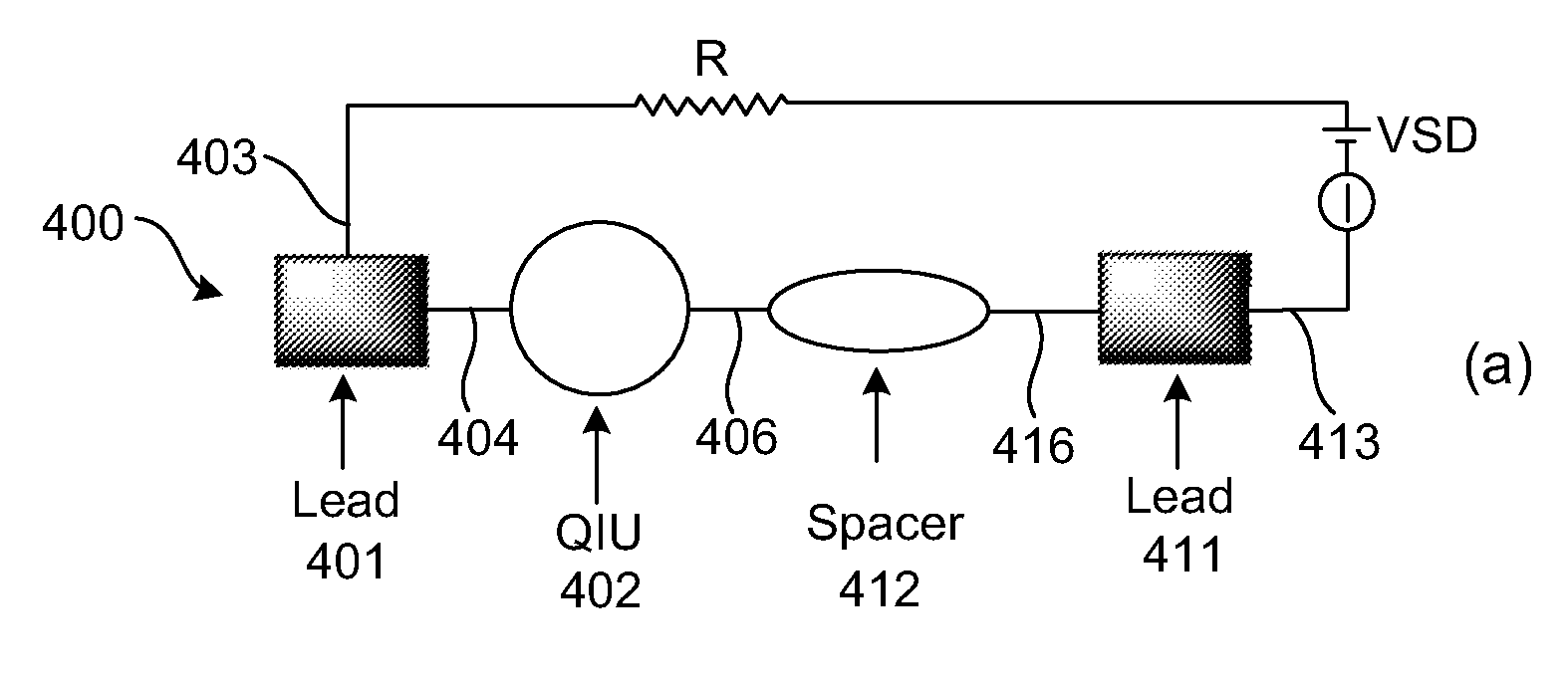
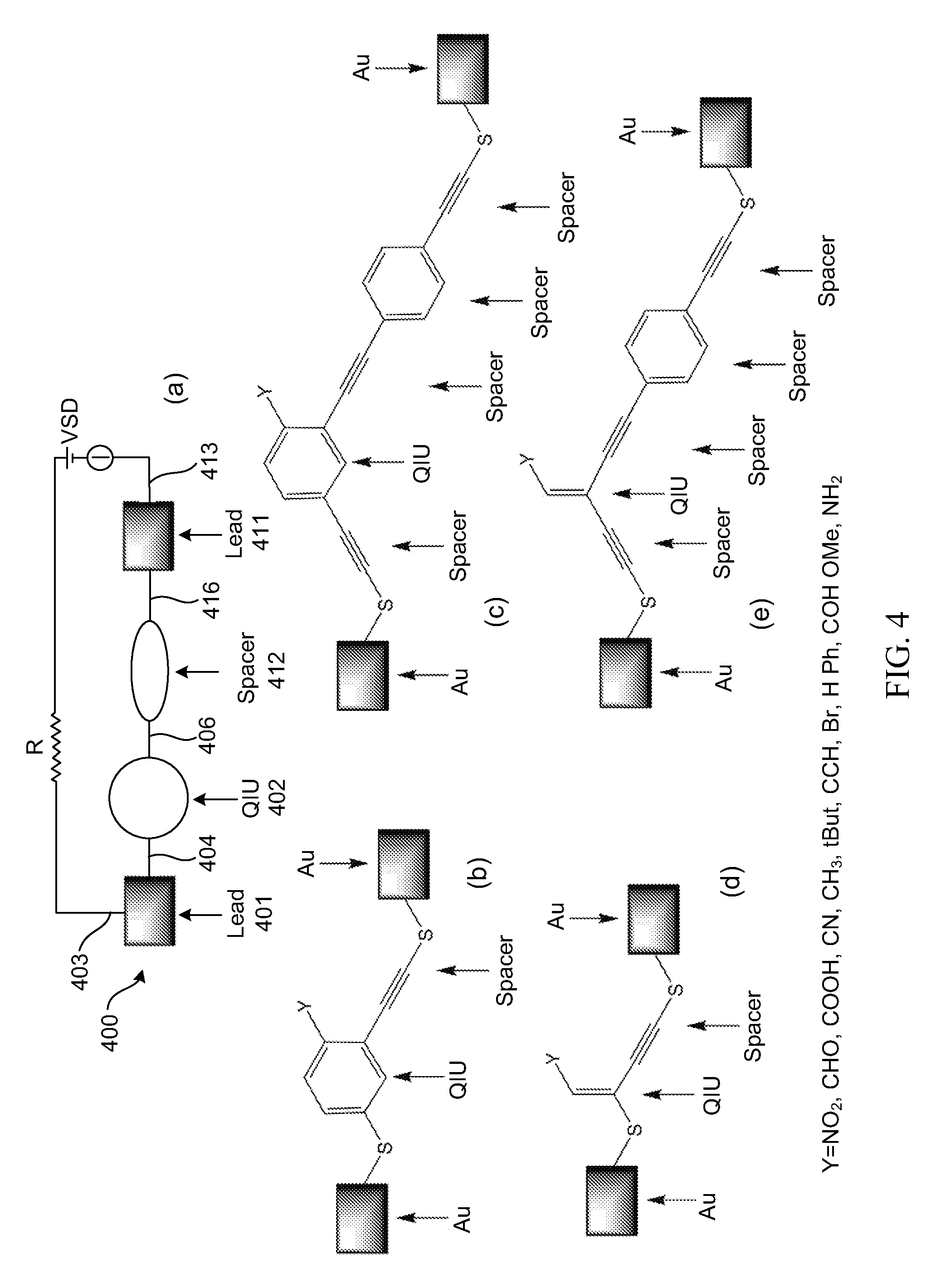
[0029]In another embodiment, the at least two molecular quantum interference units comprise at least one more molecular quantum interference unit coupled between the at least one molecular spacer and one of the first electrode and the second electrode.

Problems solved by technology

All of the molecular devices proposed and measured to date hint at the wide variety of electronic functions that can be completed within a single molecule.31 Major drawbacks in comparison with solid state devices include the low dynamic range in transport through single molecules and in the vibronic mechanisms29 that result in slow switching speed.
Therefore, a heretofore unaddressed need exists in the art to address the aforementioned deficiencies and inadequacies.

Method used


Image

  • Molecular quantum interference apparatus and applications of same
  • Molecular quantum interference apparatus and applications of same
  • Molecular quantum interference apparatus and applications of same

Examples


example 1

[0082]In designing a single molecule electronic device, it is helpful to ask what transport behavior is necessary for a molecule to function as an ideal transistor (switch), memory element, or a chemical sensor. In this exemplary embodiment of the present invention, a molecular switch is described. FIG. 11 shows the conductance of such a single-channel device with a well defined on state and off state. The line at a lower position indicates a perfect insulator. The line at 1 G0 indicates a perfect conductor representing ballistic single-channel transport, where the probability of back electron scattering within the molecule is zero. This limit of 1 G0, is a direct result from quantum theory,36,37 which has been measured in chains of Au atoms38,39 at high bias of 2 Volts,40,41 and has been verified in computational calculations42,43 With the upper and lower bounds of conductance defined by a perfect conductor and a perfect insulator, it seems trivial that a perfect switch would be a ...

example 2

[0083]In this exemplary embodiment of the present invention, how the conductance through a molecule can switch as a function of voltage is discussed. In a two-probe single molecule junction, measurements are limited to the current as a function of voltage, along with the derivative and second derivative of the data. In charge transport calculations, we determine the transmission probability of an incident electron as a function of energy. Integration of the transmission probability over the range of chemical potentials of the left and right leads will give the current.37 The transmission plots provide more detail on the molecular causes of the I / V characteristics; therefore, the following discussion is focused on understanding and controlling the electron transmission probability.

[0084]In FIG. 12(a), the transmission through a perfect conductor is shown in red, a perfect insulator in blue, and a candidate for a molecular switch in green. This hypothetical molecule behaves as a volta...

example 3

[0085]In this exemplary embodiment of the present invention, having demonstrated what represents an ideal transmission function for a single molecule with on and off states, how this transmission function can be manipulated to achieve switching behavior is described. In a three terminal measurement, the maximum Ion / Ioff ratio for a specific molecule is defined as the transmission probability at the energetically closest frontier molecular orbital / the transmission probability at the Fermi level.44 When the incident electron energy corresponds to a molecular resonance, the elastic transmission probability is equal to or ˜1. To get a large dynamic range, one needs to have molecular systems where the transmission probability also goes to zero. A molecular insulator has a very low conductance state at the Fermi level and the energetically closest resonance should have a transmission probability of 1. This would indicate that an imperfect molecular insulator might be an ideal electronic d...


PUM


Abstract

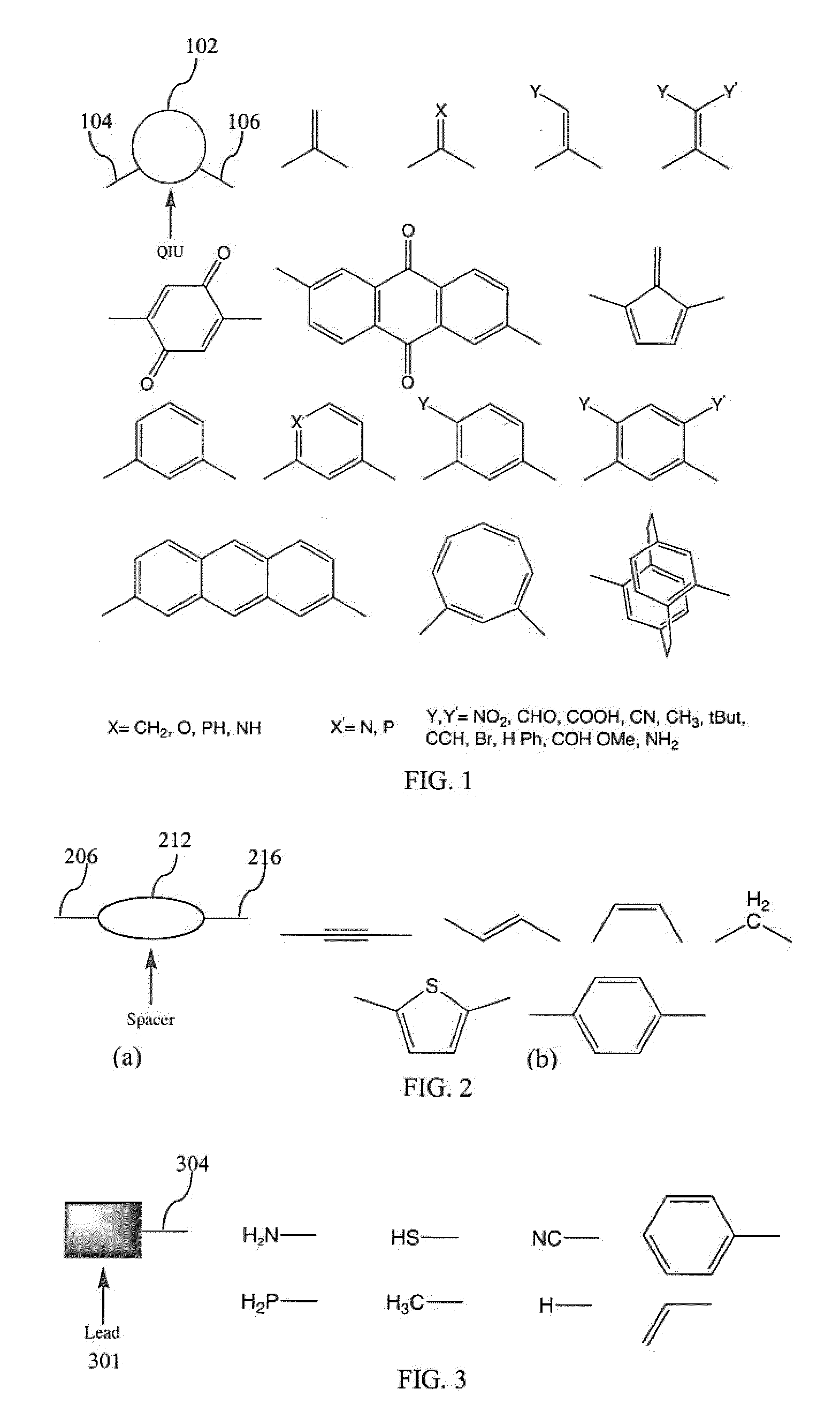
A molecular quantum interference device for use in molecular electronics. In one embodiment, the device includes a molecular quantum interference unit having a first terminal group and a second terminal group between which quantum interference affects electrical conduction, a molecular spacer having a first terminal group and a second terminal group and coupled to the molecular quantum interference unit through a chemical bonding between the first terminal group of the molecular spacer and the second terminal group of the molecular quantum interference unit, a first electrode electrically coupled to the molecular quantum interference unit and configured to supply charge carriers to or receive charge carriers from the molecular quantum interference unit, and a second electrode electrically coupled to the molecular spacer and configured to receive charge carriers from or supply charge carriers to the molecular spacer.

Description

CROSS-REFERENCE TO RELATED PATENT APPLICATION[0001]This application claims the priority to and benefit of, pursuant to 35 U.S.C. §119(e), U.S. provisional patent application Ser. No. 61 / 014,563, filed Dec. 18, 2007, entitled “MOLECULAR QUANTUM INTERFERENCE APPARATUS AND APPLICATIONS OF SAME,” by Solomon et al., which is incorporated herein by reference in its entirety.[0002]Some references, which may include patents, patent applications and various publications, are cited and discussed in the description of this invention. The citation and / or discussion of such references is provided merely to clarify the description of the present invention and is not an admission that any such reference is “prior art” to the invention described herein. All references cited and discussed in this specification are incorporated herein by reference in their entireties and to the same extent as if each reference was individually incorporated by reference.STATEMENT OF FEDERALLY-SPONSORED RESEARCH[0003]T...

Claims


Application Information

Patent Timeline
Patent Type & Authority Applications(United States)
IPC IPC(8): H01L29/12
CPCB82Y10/00G11C13/0014H01L51/0595H01L51/0591G11C13/02H10K10/701H10K10/50
Inventor SOLOMON, GEMMAANDREWS, DAVID
Owner NORTHWESTERN UNIV
Learn More