

Phase change memory element and method for forming the same
- Summary
- Abstract
- Description
- Claims
- Application Information
AI Technical Summary
Benefits of technology
Problems solved by technology
Method used
Image

Examples
Embodiment Construction
[0019]The following description is of the best-contemplated mode of carrying out the invention. This description is made for the purpose of illustrating the general principles of the invention and should not be taken in a limiting sense. The scope of the invention is best determined by reference to the appended claims.
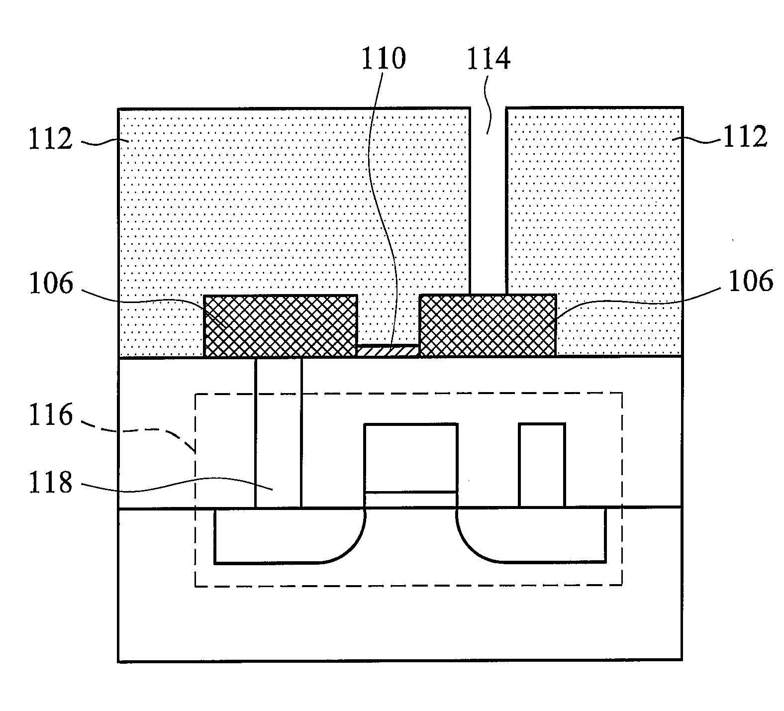
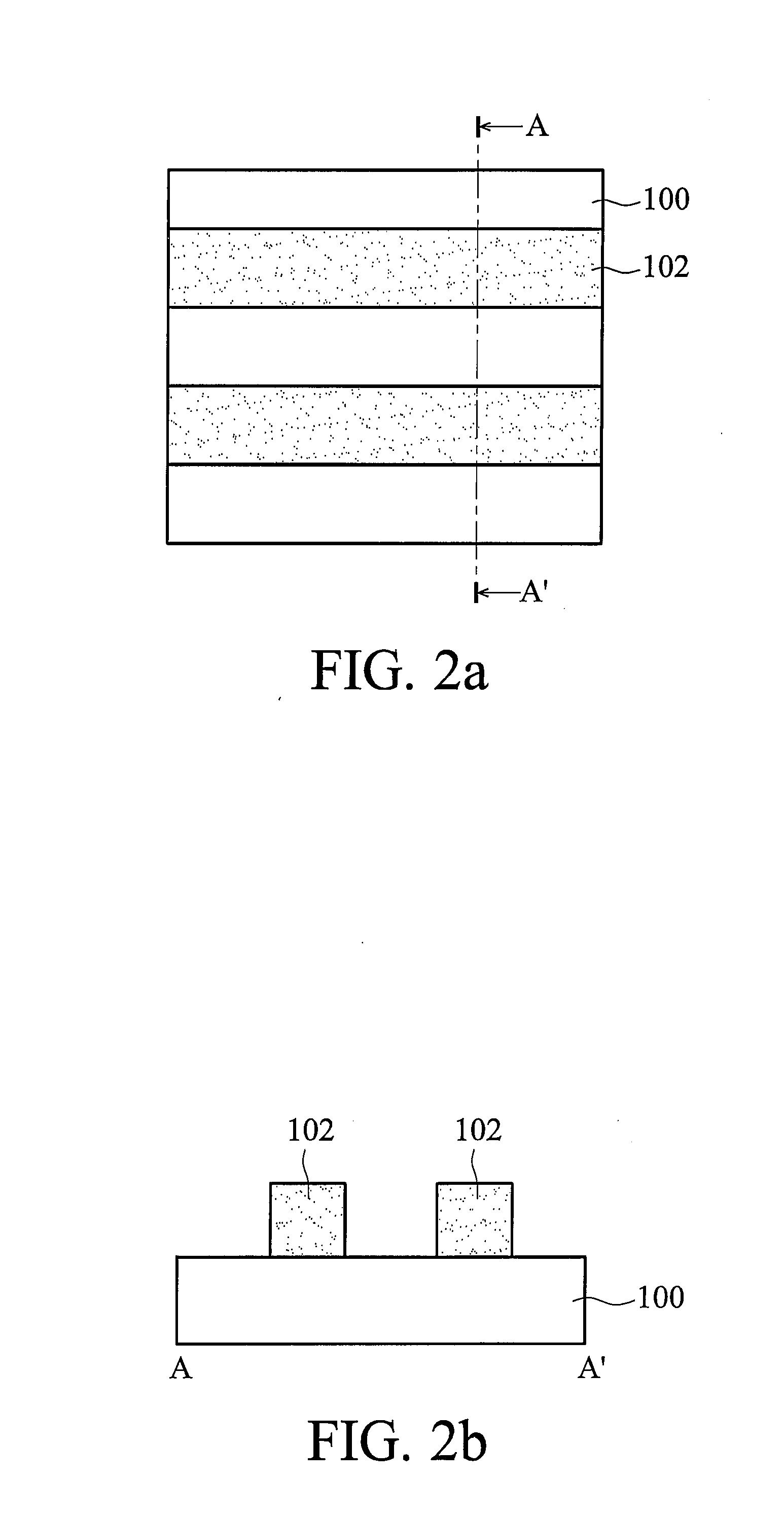
[0020]First, referring to FIG. 2a, a substrate 100 with a plurality of rectangle-shaped dielectric patterns 102 formed thereon is provided, exposing parts of surface of the substrate. Particularly, the substrate 100 can be a substrate employed in a semiconductor process, such as silicon substrate. The substrate 100 can be a substrate including a complementary metal oxide semiconductor (CMOS) circuit, isolation structure, diode, or capacitor. The accompanying drawings show the substrate 100 in a plain rectangle in order to simplify the illustration. Suitable material for the dielectric patterns can be silicon-containing material, such as silicon oxide or silicon nitride...
PUM
 Abstract
Description
Claims
Application Information