Simultaneous buried strap and buried contact via formation for soi deep trench capacitor

Inactive Publication Date: 2009-10-08
IBM CORP
View PDF5 Cites 35 Cited by
  • Summary
  • Abstract
  • Description
  • Claims
  • Application Information

AI Technical Summary

Benefits of technology

[0031]a field effect transistor located in the top semiconductor layer, wherein a source region of the field effect transistor late

Problems solved by technology

In an SOI substrate, however, the presence of the buried insulator layer prevents formation of such a rea

Method used


Image

  • Simultaneous buried strap and buried contact via formation for soi deep trench capacitor
  • Simultaneous buried strap and buried contact via formation for soi deep trench capacitor
  • Simultaneous buried strap and buried contact via formation for soi deep trench capacitor

Examples


Embodiment Construction

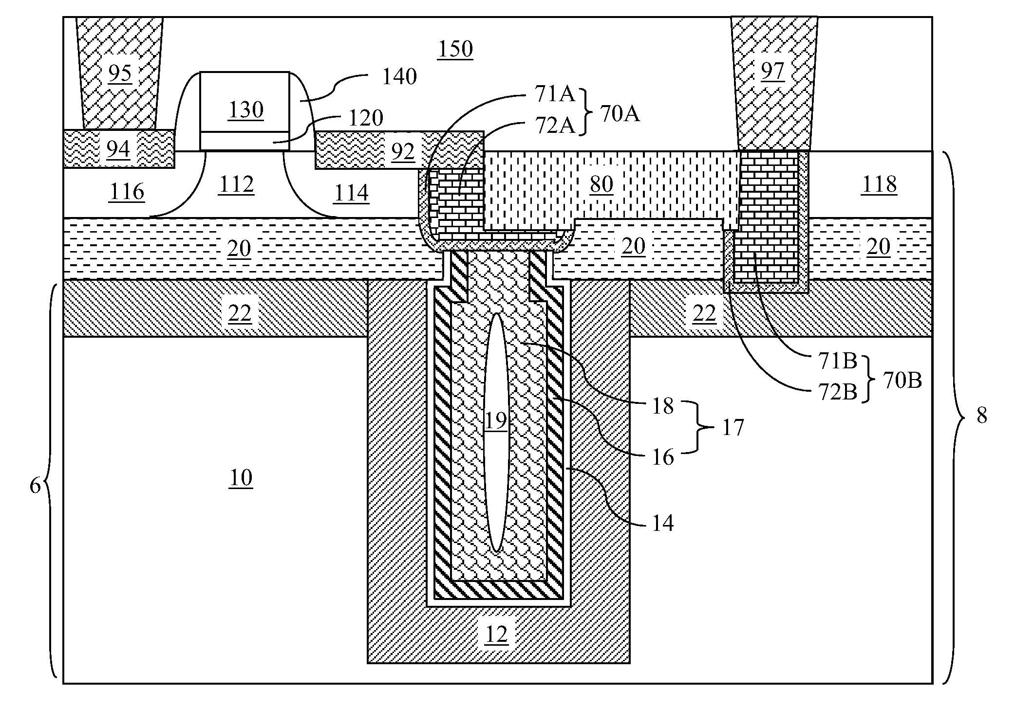
[0047]As stated above, the present invention relates to a deep trench capacitor in a semiconductor-on-insulator (SOI) substrate including a buried strap and a buried layer contact and methods of manufacturing the same, which are now described in detail with accompanying figures. It is noted that like reference numerals refer to like elements across different embodiments.

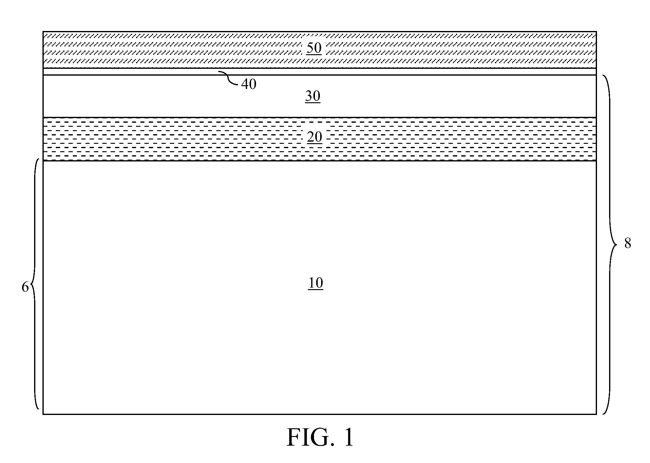
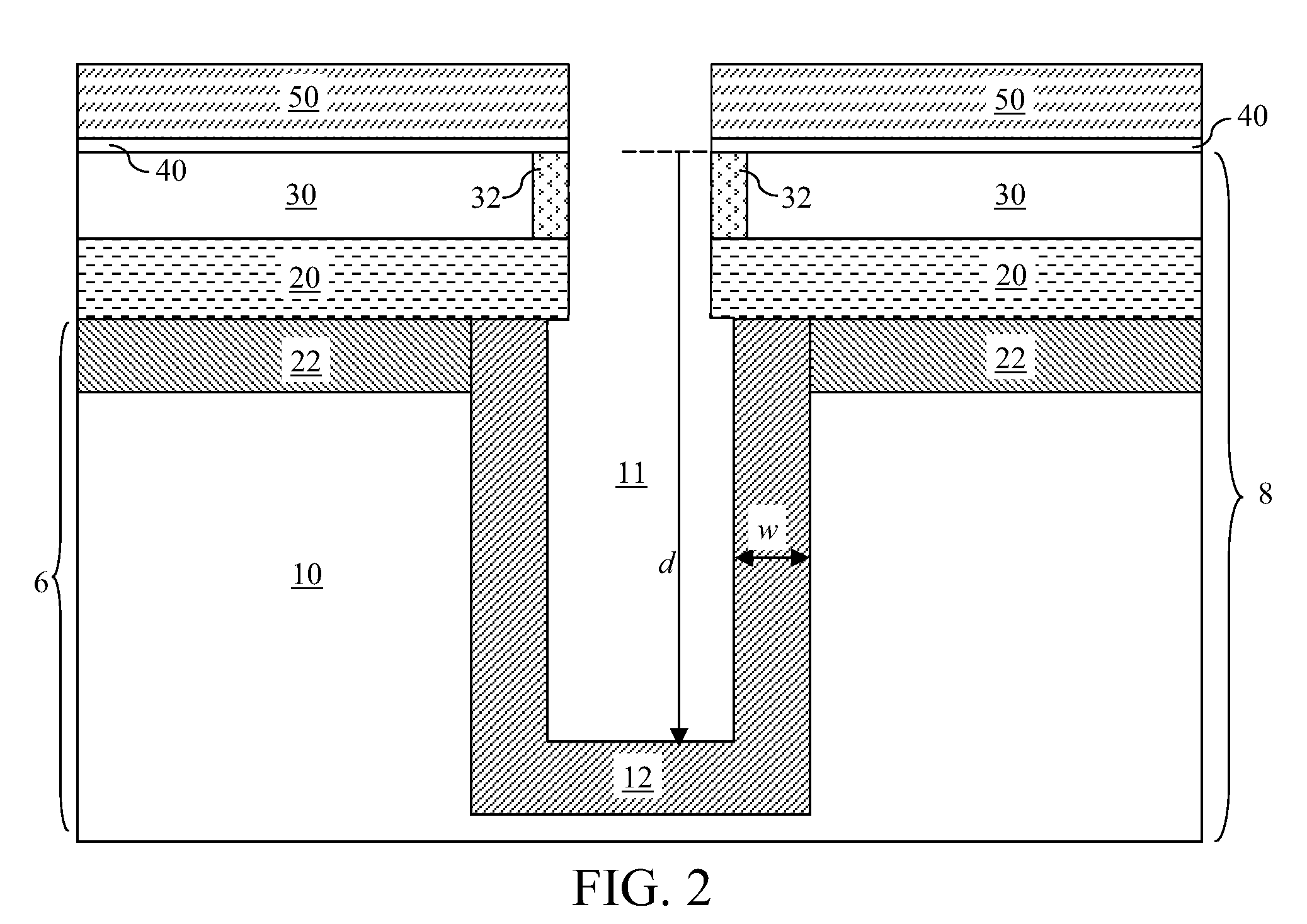
[0048]Referring to FIG. 1, an exemplary semiconductor structure according to the present invention comprises a semiconductor-in-insulator (SOI) substrate 8 containing a top semiconductor layer 30, a buried insulator layer 20, and a bottom semiconductor layer 6. Each of the top semiconductor layer 30 and the bottom semiconductor layer 6 comprises a semiconductor material. The semiconductor material of the top semiconductor layer 30 and the semiconductor material of the bottom semiconductor layer 6 may be the same, or different. The semiconductor material for the top semiconductor layer 30 and the bottom semiconductor ...


PUM


Abstract

A node dielectric, an inner electrode, and a buried strap cavity are formed in the deep trench in an SOI substrate. A buried layer contact cavity is formed by lithographic methods. The buried strap cavity and the buried layer contact cavity are filled simultaneously by deposition of a conductive material, which is subsequently planarized to form a buried strap in the deep trench and a buried contact via outside the deep trench. The simultaneous formation of the buried strap and the buried contact via enables formation of a deep trench capacitor in the SOI substrate in an economic and efficient manner.

Description

FIELD OF THE INVENTION[0001]The present invention relates to a semiconductor structure, and particularly to a deep trench capacitor in a semiconductor-on-insulator (SOI) substrate including a buried strap and a buried layer contact, and methods of manufacturing the same.BACKGROUND OF THE INVENTION[0002]Deep trench capacitors are used in a variety of semiconductor chips for high areal capacitance and low device leakage. Typically, a deep trench capacitor provides a capacitance in the range from about 4 fF to about 120 fF. A deep trench capacitor may be employed as a charge storage unit in a dynamic random access memory (DRAM), which may be provided as a stand-alone semiconductor chip, or may be embedded in a system-on-chip (SoC) semiconductor chip. A deep trench capacitor may also be employed in a variety of circuit applications such as a charge pump or a capacitive analog component in a radio-frequency (RF) circuit.[0003]Semiconductor-on-insulator (SOI) devices formed on an SOI subs...

Claims


Application Information

Patent Timeline
IPC IPC(8): H01L29/94H01L21/8242
CPCH01L21/84H01L29/66181H01L27/1203H01L27/10867H01L21/76895H01L21/743H10B12/0385
Inventor DYER, THOMAS W.
Owner IBM CORP
Why Eureka
Try Eureka