Circuit complexity reduction of a capacitive touch system

a capacitive touch and circuit complexity technology, applied in the field of capacitive touch system structure, can solve the problems of reducing the frame rate of unable to implement multi-finger touch detection, and affecting the overall touch panel application, so as to reduce the number of required pins, and reduce the frame rate

Inactive Publication Date: 2009-10-08
ELAN MICROELECTRONICS CORPORATION
View PDF19 Cites 17 Cited by
  • Summary
  • Abstract
  • Description
  • Claims
  • Application Information

AI Technical Summary

Benefits of technology

[0005]An object of the present invention is to provide a capacitive touch system applicable to large scale touch panels with a multi-finger touch detection, a good frame rate, and low circuit complexity.
[0006]According to the present invention, a capacitive touch system uses at least two first integrated circuits to simultaneously scan a touch panel, each of the first integrated circuits responsible for scanning only a respective portion of the touch panel. The first integrated circuits transmit their sensed data to a second integrated circuit where a calculation with the received sensed data is executed. Alternatively, each or any of the first integrated circuits may share a calculation with its sensed data or all the sensed data. In addition, the second integrated circuit may also participate in scanning for a respective portion of the touch panel. Each of the first integrated circuits has at least a pin to transmit its sensed data, and the second integrated circuit has at least a common pin connected to the at least a pin of each of the first integrated circuits to receive the sensed data therefrom. This structure reduces the number of required pins of the second integrated circuit and thereby lowers the overall circuit complexity.

Problems solved by technology

In a two dimensional matrix for instance, only one set of parameters (X,Y) will be determined, and thereby it can't implement a multi-finger touch detection.
An all points addressable (APA) projected capacitance sensing technique is capable of implementing a multi-finger touch detection, but not applicable to large scale touch panels because, to implement this sensing technique, it is necessary to charge and discharge each point sensor on the large scale touch panel.
Taking a matrix-type touch panel for example, when the X and Y traces increase, the pixel number of an APA projected capacitance touch panel dramatically increases and thereby significantly degrades the frame rate of the touch panel due to the very long time period for scanning the large scale touch panel in a frame.
Unfortunately, the frame rate of the overall touch panel application is dependent to a very large extent on the time it takes the touch IC 12 to charge and discharge capacitors each time.
Hence, if an AI projected capacitance touch IC capable of scanning a greater number of traces is applied to a large scale touch panel 14, a major drawback would be a significantly decreased frame rate in the overall application, which leads to compromised performance at the application end.

Method used


Image

  • Circuit complexity reduction of a capacitive touch system
  • Circuit complexity reduction of a capacitive touch system
  • Circuit complexity reduction of a capacitive touch system

Examples


first embodiment

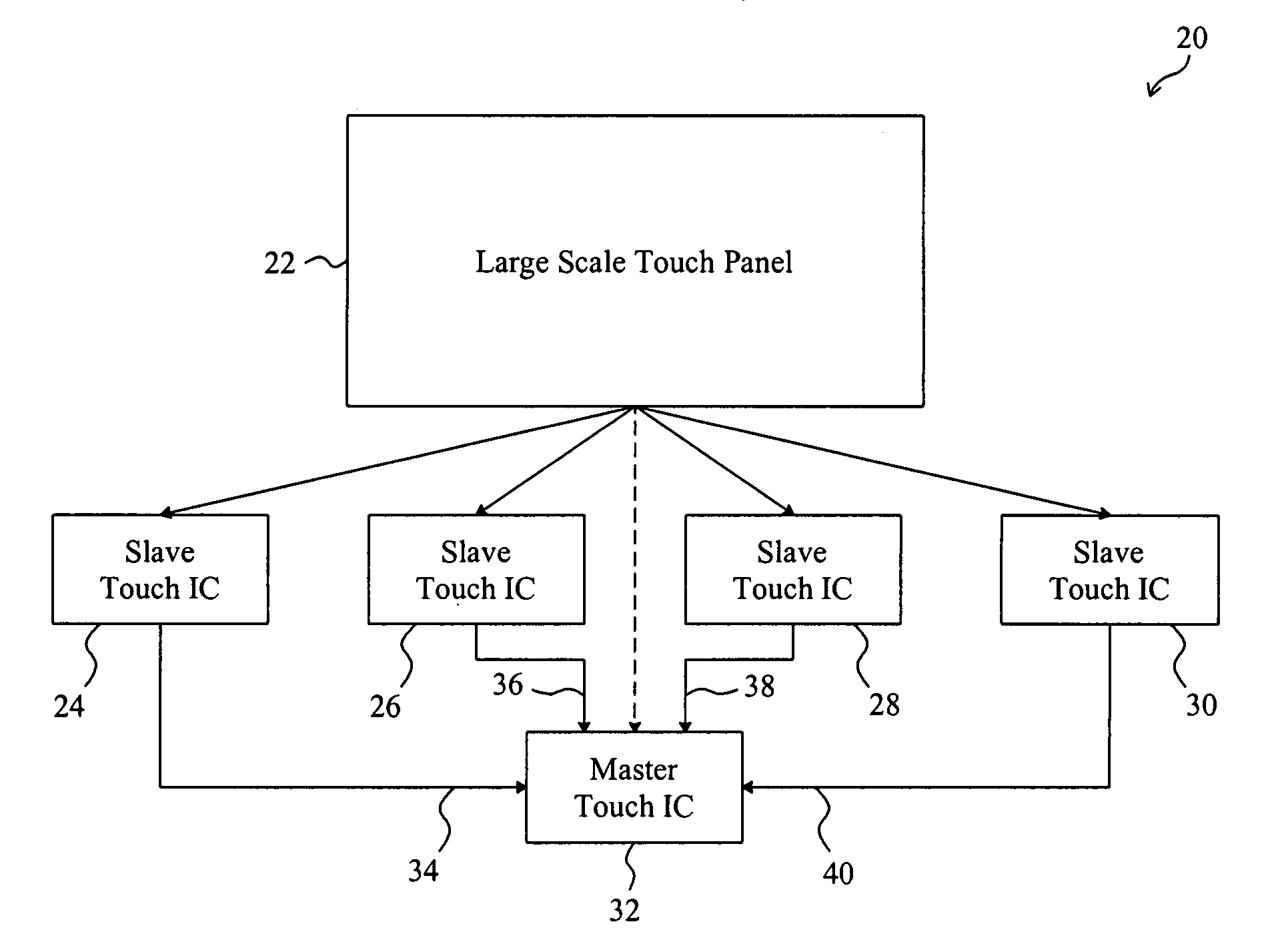
[0016]FIG. 4 is a schematic diagram of a first embodiment according to the present invention, in which a capacitive touch system 50 includes four AI projected capacitance touch ICs 52, 54, 56 and 58 as the slave touch ICs to scan a touch panel (not shown) and for their sensed data, transmit with serial data to a master touch IC 60 in a serial transmission mode, as does a serial port. Each of the slave touch ICs 52-58 has two pins CLKS and SDAS, the pins SDAS of all the slave touch ICs 52-58 are connected together to a common pin SDAM of the master touch IC 60, and the pins CLKS of all the slave touch ICs 52-58 are connected together to a common pin CLKM of the master touch IC 60: This structure may reduce the number of pins of the master touch IC 60. The master touch IC 60 sends out a clock to the pin CLKS of each of the slave touch ICs 52-58 via the common pin CLKM, and receives the sensed data from each of the slave touch ICs 52-58 via the common pin SDAM. The master touch IC 60 f...

second embodiment

[0017]FIG. 5 is a schematic diagram of a second embodiment according to the present invention, in which a capacitive touch system 70 has much more slave touch ICs 72-82, also configured with a serial transmission scheme, for example, as that shown in FIG. 4. The number of the total slave touch ICs 72-82 is 2N, where N is a natural number. Each of the slave touch ICs 72-82 is an AI projected capacitance touch IC, and is responsible for scanning a respective portion of a touch panel (not shown). All the slave touch ICs 72-82 transmit their sensed data to a master touch IC 84 in a serial transmission mode, as does a serial port. Each of the slave touch ICs 72-82 has two pins CLKS and SDAS, all the pins SDAS are connected together to a common pin SDAM of the master touch IC 84, and all the pins CLKS are connected together to a common pin CLKM of the master touch IC 84. The master touch IC 84 sends out a clock to the pin CLKS of each of the slave touch ICs 72-82 via the common pin CLKM, ...

third embodiment

[0018]FIG. 6 is a schematic diagram of a third embodiment according to the present invention, in which each of slave touch ICs 72-82 transmits its sensed data to a master touch IC 84 in a parallel transmission mode to increase the data transmission speed. The number of the slave touch ICs 72-82 in this capacitive touch system 90 is also 2N, where N is a natural number. For each of the slave touch ICs 72-82, the number of pins to transmit its sensed data is M, where M is a natural number, and the sensed data will be transmitted with a data width of M. To reduce the number of pins of the master touch IC 84, the pins SDAS[M−1:0] of all the slave touch ICs 72-82 are connected together to common pins SDAM[M−1:0] of the master touch IC 84, the pins CLKS of all the slave touch ICs 72-82 are connected together to a common pin CLKM of the master touch IC 84 to receive a clock therefrom, and the master touch IC 84 also sends out an address signal Addr[N−1:0] to select from the slave touch ICs...


PUM


Abstract

A capacitive touch system uses at least two first integrated circuits to simultaneously scan a touch panel, each of the first integrated circuits only for scanning a portion of the touch panel. Therefore, the capacitive touch system can maintain a good frame rate, even the touch panel is a large scale touch panel. Each of the first integrated circuits transmits its sensed data to a second integrated circuit where a calculation with the received sensed data is executed. The second integrated circuit has at least a common pin connected to each of the first integrated circuits, and therefore the number of pins of the second integrated circuit is reduced.

Description

FIELD OF THE INVENTION[0001]The present invention is related generally to a capacitive touch system and, more particularly, to a structure for circuit complexity reduction of a capacitive touch system.BACKGROUND OF THE INVENTION[0002]In conventional applications, all the large scale capacitive touch panels use a surface capacitance sensing technique to scan thereto for determining a touch information, which uses a set of sensing currents, each directed to an endpoint of the large scale touch panel to produce sensed values, and therefore, even multiple fingers simultaneously touch the large scale touch panel, this sensing technique still retrieves only one set of sensed currents in response to this multi-finger touch. For this reason, the surface capacitance sensing technique can identify only one set of absolute coordinates. In a two dimensional matrix for instance, only one set of parameters (X,Y) will be determined, and thereby it can't implement a multi-finger touch detection.[00...

Claims


Application Information

Patent Timeline
Patent Type & Authority Applications(United States)
IPC IPC(8): G06F3/041
CPCG06F3/044G06F3/0416G06F3/04166G06F3/04164
Inventor HUNG, TSE-LUNHUANG, JUNG-SHOUCHEN, CHANG-HSIN
Owner ELAN MICROELECTRONICS CORPORATION
Why Eureka
Try Eureka