Etching process state judgment method and system therefor

Active Publication Date: 2009-10-08
HITACHI HIGH-TECH CORP
View PDF3 Cites 93 Cited by
  • Summary
  • Abstract
  • Description
  • Claims
  • Application Information

AI Technical Summary

Benefits of technology

[0008]In Patent Document 1, a peak wavelength is previously defined as a wavelength of a substance. In other words, it is judged whether a peak exists or not at the wavelength of light emitted from a certain substance. Thus, it is i

Problems solved by technology

Thus, it is impossible to detect a peak if the peak exists at a different wavelength from the wavelengths of light emitted

Method used


Image

  • Etching process state judgment method and system therefor
  • Etching process state judgment method and system therefor
  • Etching process state judgment method and system therefor

Examples


Embodiment Construction

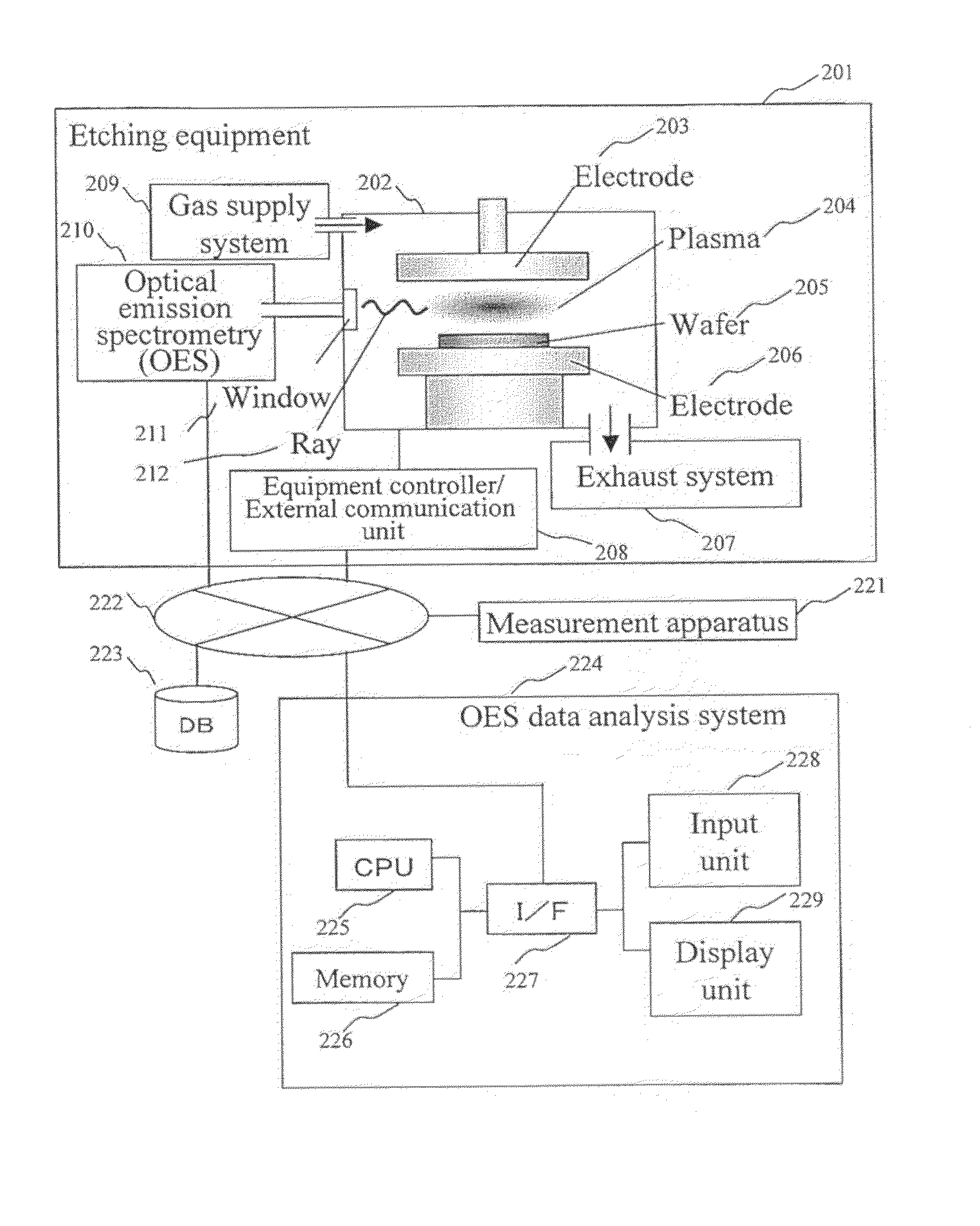
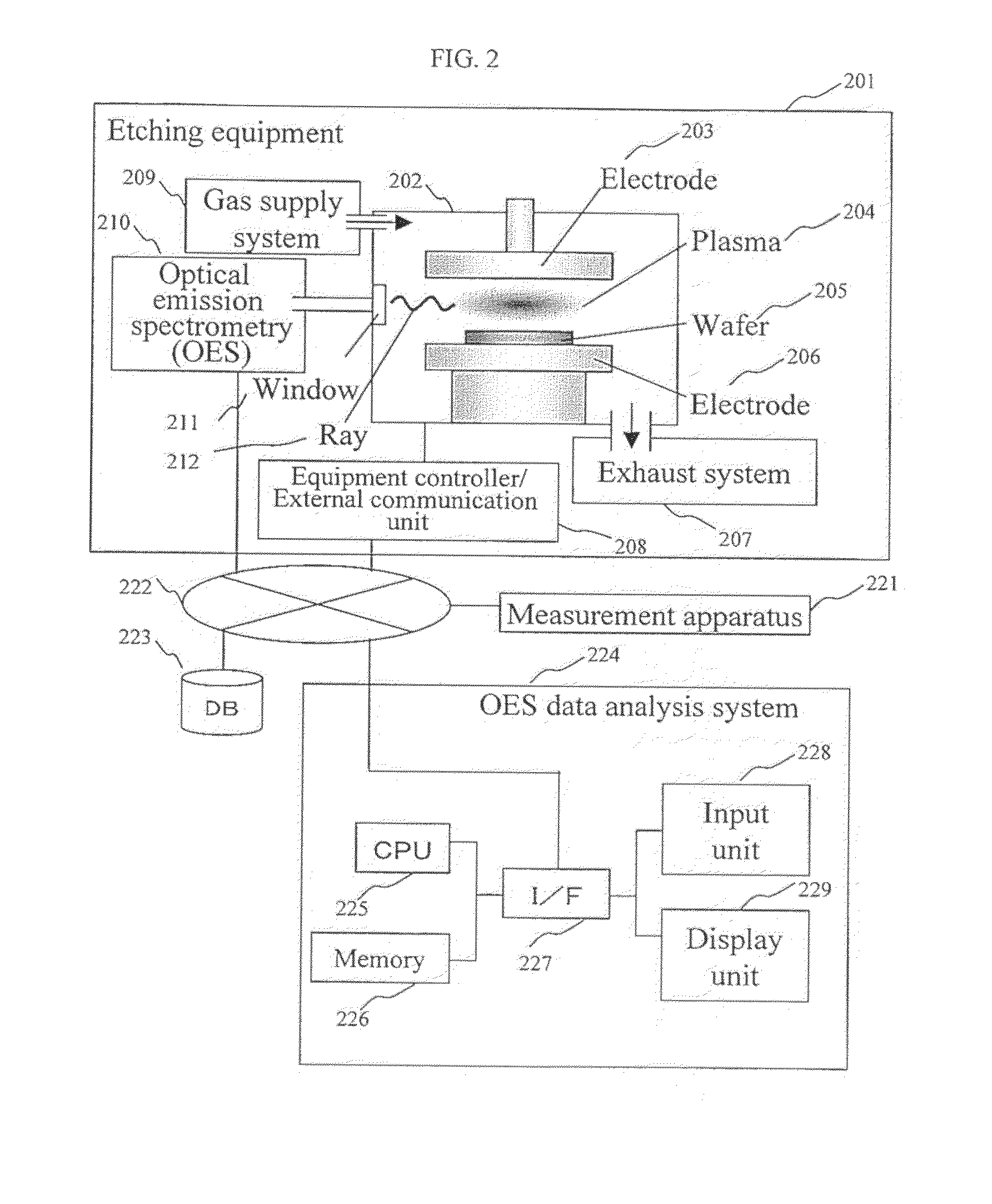
[0033]Now, one embodiment of the present invention will be described referring to the drawings.

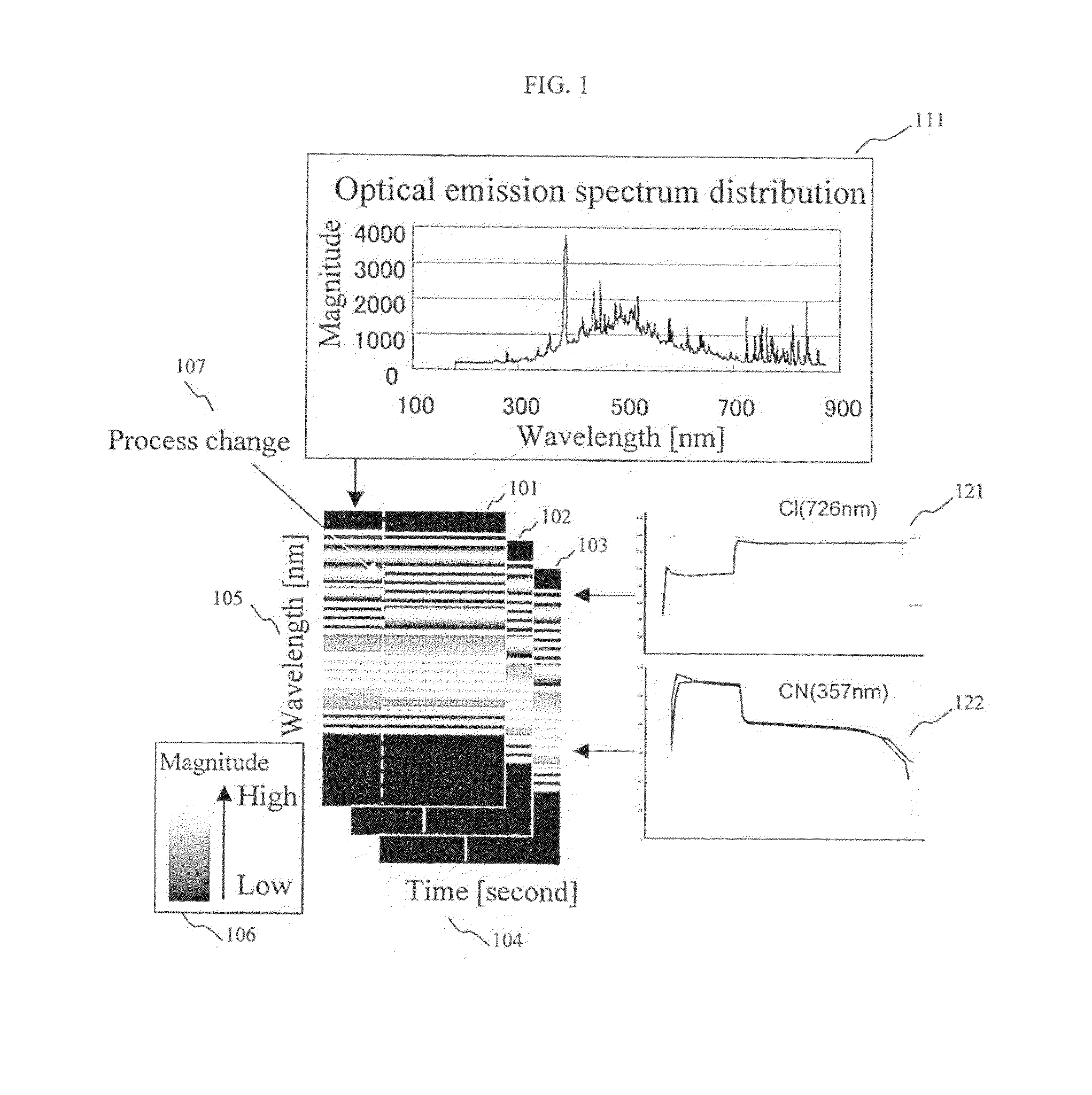
[0034]First, an optical emission spectrum distribution will be described.

[0035]FIG. 1 shows an optical emission spectrum distribution obtained by an optical emission spectrometry (OES). An optical emission spectrum distribution with time 104 on the x-axis and wavelength 105 on the y-axis can be expressed as a bitmap.

[0036]Bitmaps 101, 102 and 103 depict optical emission phenomena concerning a plurality of wafers. From an optical emission spectrum distribution 111 at a certain point of time, it is seen that the distribution is convex in the large in the neighborhood of the center of monitored wavelengths, and peaks exist at many wavelength positions.

[0037]Further, from emission magnitude (waveform) graphs 121 and 122, it is seen that the emission magnitude varies as the etching process proceeds, and the optical emission phenomenon changes at the time of process change 107.

[0038]By monitorin...


PUM

PropertyMeasurementUnit
Distributionaaaaaaaaaa

Abstract

An etching process state judgment method comprising: a spectral data obtaining step, in which an optical emission spectrum distribution is obtained by monitoring optical emission during an etching process of a plurality of wafers; a peak detection step, in which peaks are detected from the optical emission spectrum distribution at a specific time point during the etching process, to obtain peak characteristics; a common peak identifying step, in which peaks common to the wafers are identified among the peaks detected in the peak detection step; and a state detection step, in which the characteristics are compared regarding the common peaks, to detect a state of each wafer in the etching process.
A state (anomaly or normalcy) of an etching process is detected from optical emission spectrum distribution at the time of etching process, by a simple method without assuming substances.

Description

[0001]The present application claims priority from Japanese application JP 2008-098111 filed on Apr. 4, 2008, the content of which is hereby incorporated by reference into this application.BACKGROUND OF THE INVENTION[0002]The present invention relates to a technique of judging a state (anomaly or normalcy) of an etching process on the basis of optical emission spectrum distribution obtained by monitoring optical emission of plasma in etching equipment.[0003]To obtain a micro shape of a semiconductor device or the like to be formed on a wafer, an etching process is performed where a substance is ionized by using plasma, and material on the wafer is removed by action (i.e. chemical reaction on the wafer surface) of the ionized substance. Various substances may be used as the substance to be ionized, and the material on the wafer may be different according to the function of the product. Further, to form the shape on the wafer, resist of an organic substance is applied to the wafer, an...

Claims


Application Information

Patent Timeline
IPC IPC(8): H01L21/00H01L21/66
CPCG01B11/0658G01B11/0683G01B11/24G01B2210/56G01J3/443G01N21/67H01L2924/0002G01N2021/8411H01L22/26H01L2924/00
Inventor MORISAWA, TOSHIHIROIKUHARA, SHOJIKAGOSHIMA, AKIRASHIRAISHI, DAISUKE
Owner HITACHI HIGH-TECH CORP
Why Eureka
Try Eureka