Device and Method for Preventing the Influence of Conducting Material from Point Detection of Projected Capacitive Touch Panel

a capacitive touch panel and capacitive technology, applied in the field of touch panels, can solve the problems of heavy processing load, physical conditions, contact position confirmation, etc., and achieve the effect of preventing the influence of conducting material

Active Publication Date: 2009-10-15
EGALAX EMPIA TECH INC
View PDF7 Cites 57 Cited by
  • Summary
  • Abstract
  • Description
  • Claims
  • Application Information

AI Technical Summary

Benefits of technology

[0014]The present invention provides a method for preventing the influence of conducting material from point detection of projected capacitive touch panel. The method includes (a) providing a first sensing signal to a plurality of first and second axial conductive lines, wherein the first and second axial conductive lines are electrically isolated from each other; (b) sensing a plurality of second and third sensing signals simultaneously, wherein the second and the third sensing signals are correspondingly generated by the first and the second axial conductive lines receiving the first sensing signal respectively; and (c) utilizing at least one bigger change of the second and the third sensing signals respectively to match a corresponding coordinate to get the position of at least one touch point on the corresponding coordinate.
[0015]The present invention provides a method for preventing the influence of conducting material from point detection of projected capacitive touch panel. The method includes (a) providing a first sensing signal to a plurality of first and second axial conductive lines, wherein the first and second axial conductive lines are electrically isolated from each other; (b) sensing a plurality of second sensing signals; (c) sensing a plurality of third sensing signals, wherein the second and the third sensing signals are correspondingly generated by the first and the second axial conductive lines receiving the first sensing signal respectively; and (d) utilizing at least one bigger change of the second and the third sensing signals respectively to match a corresponding coordinate to get the position of at least one touch point on the corresponding coordinate.
[0016]The present invention provides a method for preventing the influence of conducting material from point detection of projected capacitive touch panel. The method includes (a) providing a first sensing signal to a plurality of first axial conductive lines, wherein the first axial conductive lines are electrically isolated from each other; (b) sensing a plurality of second sensing signals of the first axial conductive lines and a plurality of third sensing signals of a plurality of second axial conductive lines, wherein the second axial conductive lines are electrically isolated from each other and are isolated from the first axial conductive lines, the second and the third sensing signals are correspondingly generated by the first and the second axial conductive lines receiving the first sensing signal and capacitively coupling the second sensing signals respectively; and (c) utilizing at least one bigger change of the second and the third sensing signals respectively to match a corresponding coordinate to get the position of at least one touch point on the corresponding coordinate.
[0017]The present invention provides a method for preventing the influence of conducting material from point detection of projected capacitive touch panel. The method includes (a) providing a first sensing signal to a plurality of first axial conductive lines, wherein the first axial conductive lines are electrically isolated from each other; (b) sensing a plurality of second sensing signals of the first axial conductive lines; (c) sensing a plurality of third sensing signals of a plurality of second axial conductive lines, wherein the second axial conductive lines are electrically isolated from each other and are isolated from the first axial conductive lines, the second and the third sensing signals are correspondingly generated by the first and the second axial conductive lines receiving the first sensing signal and capacitively coupling the second sensing signals respectively; and (d) utilizing at least one bigger change of the second and the third sensing signals respectively to match a corresponding coordinate to get the position of at least one touch point on the corresponding coordinate.
[0018]The present invention provides a method for preventing the influence of conducting material from point detection of projected capacitive touch panel. The method includes (a) providing a first sensing signal to a plurality of first axial conductive lines, wherein the first axial conductive lines are electrically isolated from each other; (b) sensing a plurality of second sensing signals of a plurality of second axial conductive lines, wherein the second axial conductive lines are electrically isolated from each other and are isolated from the first axial conductive lines; (c) sensing a plurality of third sensing signals of the first axial conductive lines, wherein the second sensing signals are correspondingly generated by the second axial conductive lines capacitively coupling the third sensing signals, the third sensing signals are correspondingly generated by the first axial conductive lines receiving the first sensing signal; and (d) utilizing at least one bigger change of the second and the third sensing signals respectively to match a corresponding coordinate to get the position of at least one touch point on the corresponding coordinate.

Problems solved by technology

In terms of resistive touch technology, the techniques from pressing a touch screen to the contact detection, data operations, and the contact position confirmed have the technical limitations from the physical conditions.
This causes a heavy load to the processor.
So the performance of the transparency is getting worse with the use of time and frequency.
As for contact detection, some specific areas will be worn by excessively use, and thus, the conduction efficiency of an ITO conductive film is reduced.
Besides, the ITO conductive film must reserve borders, and thus the optional of the industrial design is restricted.
Still, the resistive touch technology is unable to achieve approach sense (fingers approach but not touch), as well as more difficult to deal with multi-touch.
However, the surface capacitive touch technology has the problem of hand-shadow effect.
That is, when a surface capacitive touch screen is active, if user's wrist and fingers approach the screen surface together, it will make the surface of the ITO conductive film and the inside of the screen generate excessive charges.
These excessive charges lead to produce coupling capacitance and make the surface capacitive touch screen sense error.
Also, because the surface capacitive technology senses the contact by the change of the electric field, the accuracy of contact detection will be affected when the use of environment has the problem of electromagnetic interference.
This change makes the measuring control circuit, such as sensing unit 160, sense the current change or charge change on the axial conductive lines, and then results in misjudgment and mal-operation.
Therefore, the position of the touch point TP cannot be correctly sensed.

Method used


Image

  • Device and Method for Preventing the Influence of Conducting Material from Point Detection of Projected Capacitive Touch Panel
  • Device and Method for Preventing the Influence of Conducting Material from Point Detection of Projected Capacitive Touch Panel
  • Device and Method for Preventing the Influence of Conducting Material from Point Detection of Projected Capacitive Touch Panel

Examples


Embodiment Construction

[0029]Some embodiments of the present invention will now be described in greater detail. Nevertheless, it should be noted that the present invention can be practiced in a wide range of other embodiments besides those explicitly described, and the scope of the present invention is expressly not limited except as specified in the accompanying claims.

[0030]Moreover, some irrelevant details are not drawn in order to make the illustrations concise and to provide a clear description for easily understanding the present invention.

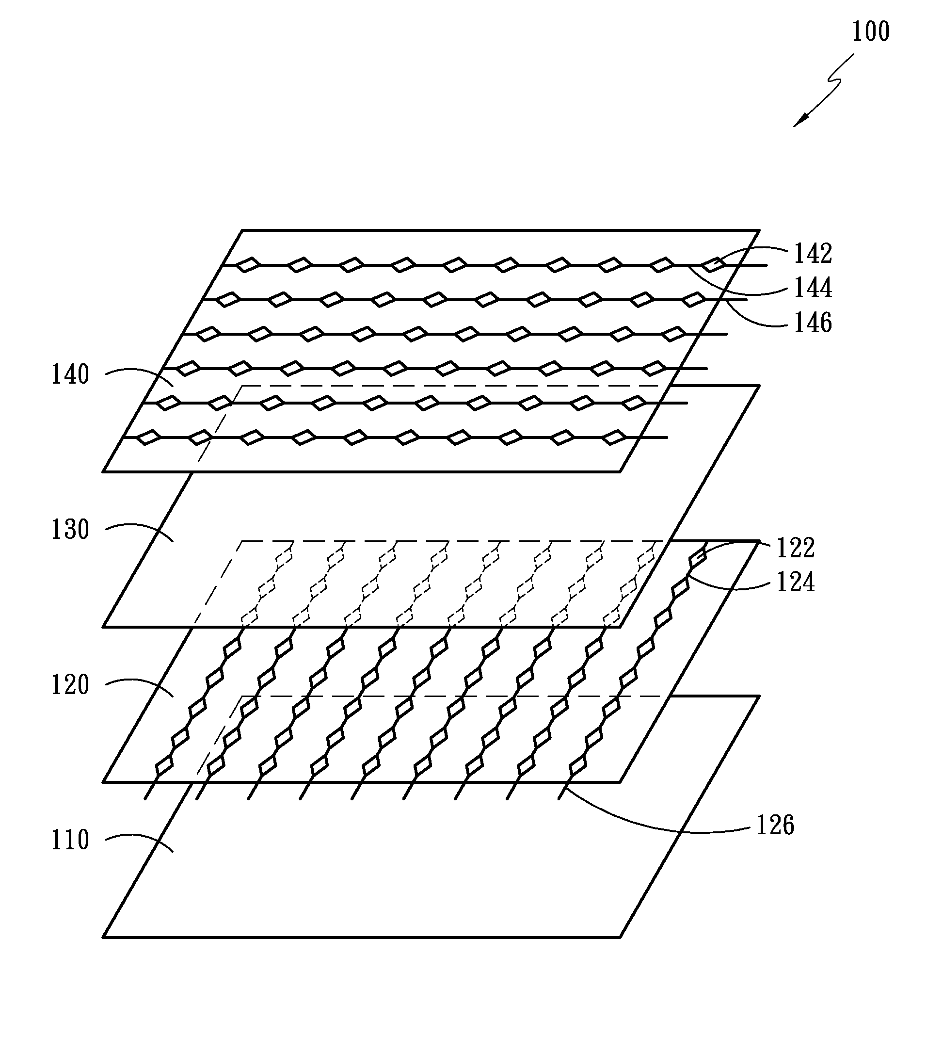
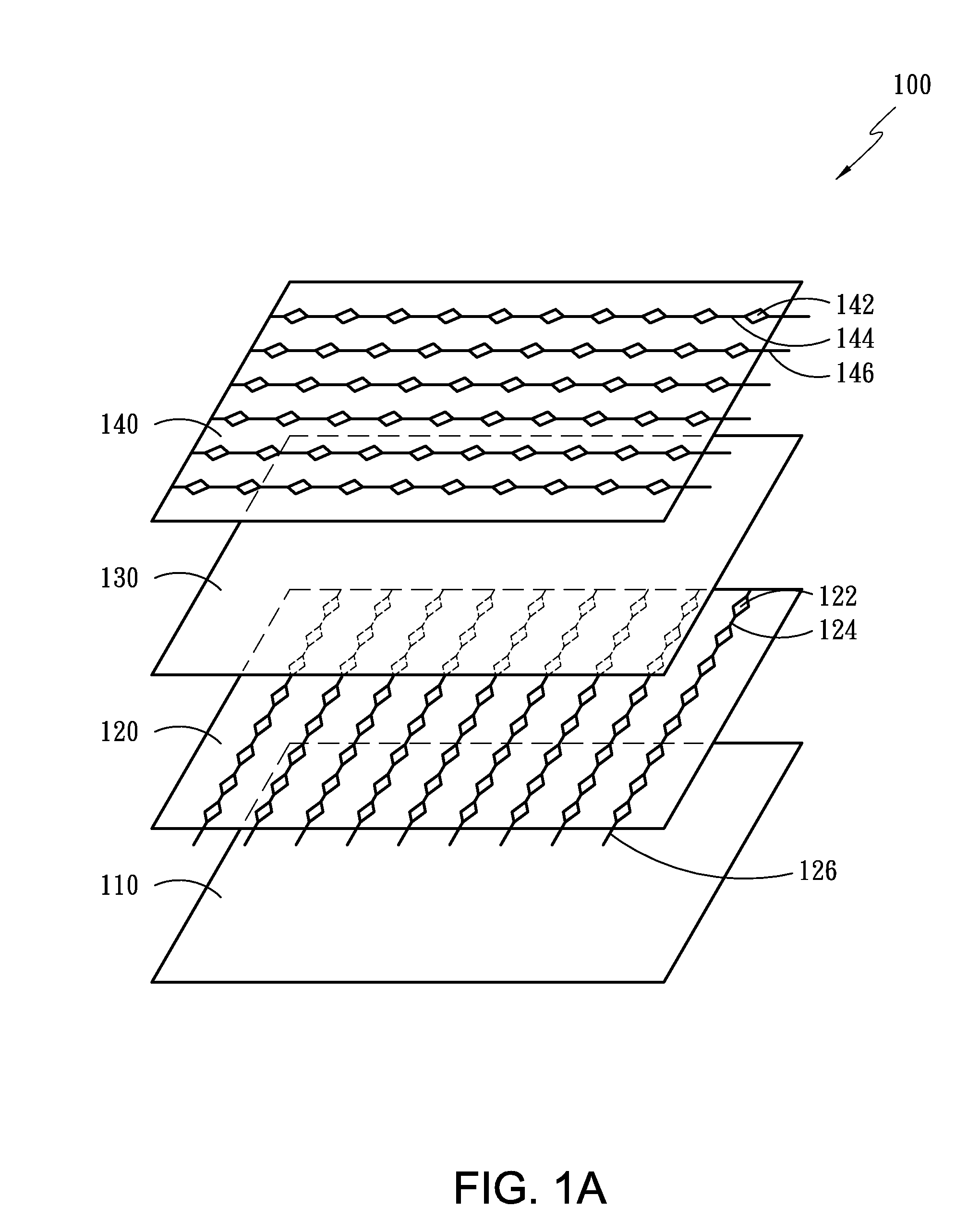
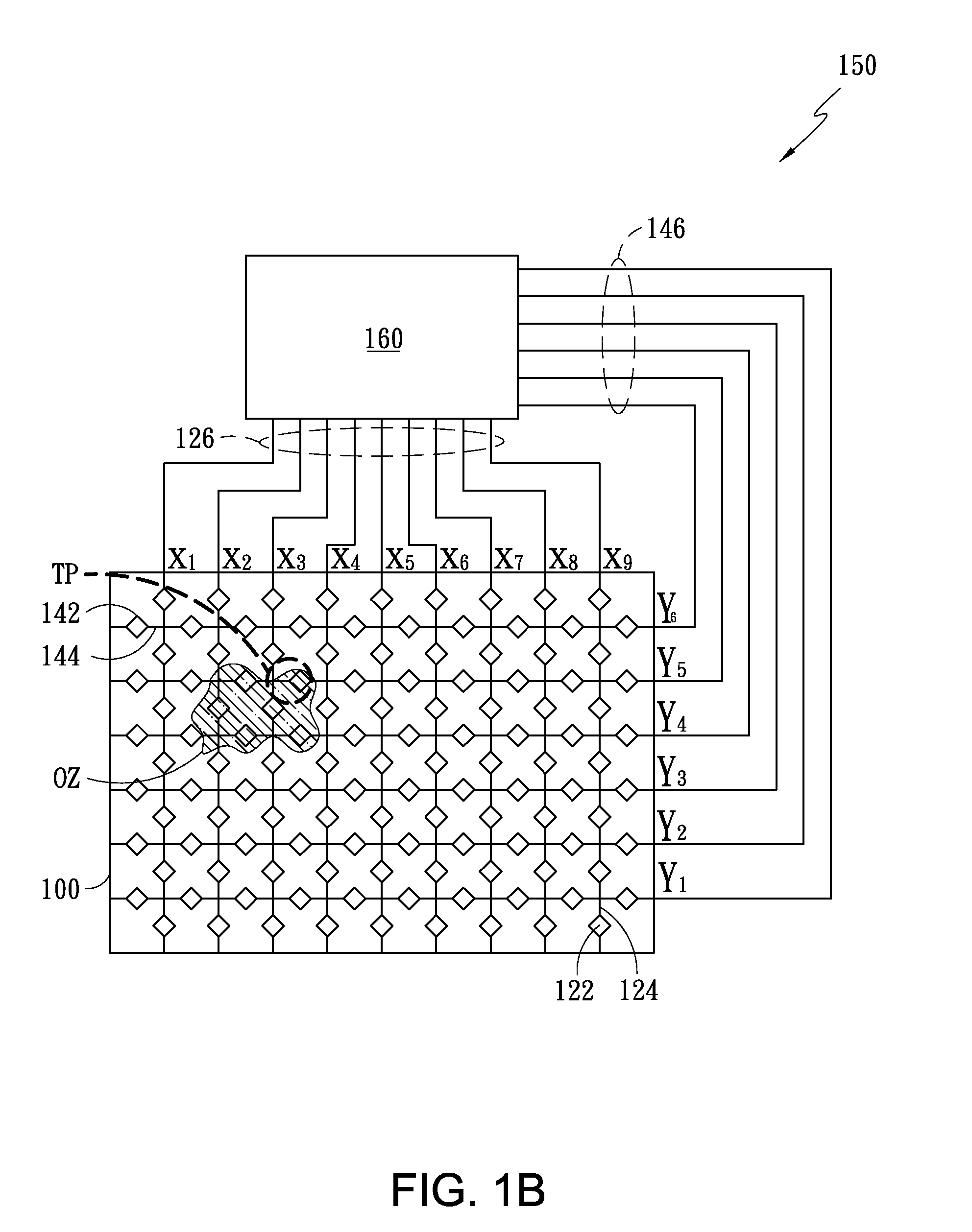
[0031]Referring to FIG. 2A, an active circuit 200 of one preferred embodiment in accordance with the present invention is depicted. A projected capacitive touch panel 100 (referring to FIG. 1A) at least includes a first sensing layer 120 and a second sensing layer 140. The first sensing layer 120 has a plurality of first axial conductive lines 124 isolated from each other and correspondingly electrically connected to a plurality of first outside-connection conduct...


PUM


Abstract

This invention provides a device for preventing the influence of conducting material from point detection of projected capacitive touch panel. The device includes a first sensing layer having a plurality of first axial conductive lines isolated from each other and electrically connected to a plurality of first outside-connection conducting wires correspondingly, a second sensing layer having a plurality of second axial conductive lines isolated from each other and electrically connected to a plurality of second outside-connection conducting wires correspondingly, a signal driving line electrically connecting to the first and the second outside-connection conducting wires to provide a first sensing signal, and a sensing unit electrically connecting the first and the second outside-connection conducting wires to sense the sensing signal on the first and the second axial conductive lines. Wherein, the second sensing layer is on a dielectric layer, the first sensing layer, and a substrate in sequence.

Description

BACKGROUND OF THE INVENTION[0001]1. Field of the Invention[0002]This invention generally relates to the field of touch panel, and more particularly, to a device and method for preventing the influence of conducting material from point detection of projected capacitive touch panel.[0003]2. Description of the Prior Art[0004]Nowadays, the common touch technologies used by electronic devices include resistive, surface capacitive, projected capacitive, surface acoustic wave, optics imaging, infrared, bending wave, active digitizer, and so forth. Since the packaging volumes of the first three technologies are smaller, their precision can be done relatively high. And they are suitable to those smaller mobile device or portable consumer electronic products.[0005]In terms of resistive touch technology, the techniques from pressing a touch screen to the contact detection, data operations, and the contact position confirmed have the technical limitations from the physical conditions. That is, ...

Claims


Application Information

Patent Timeline
Patent Type & Authority Applications(United States)
IPC IPC(8): G08C21/00
CPCG06F3/044G06F3/0418G06F3/04186G06F3/0445G06F3/0446
Inventor CHANG, CHIN-FULIN, YU-HANLEE, CHENG-HAN
Owner EGALAX EMPIA TECH INC
Why Eureka
Try Eureka