Transistors having asymmetric strained source/drain portions

a technology of transistors and drain portions, which is applied in the direction of basic electric elements, electrical apparatus, semiconductor devices, etc., can solve the problem that the structure usually does not have the optimum strain in the channel region, and achieve the effect of higher strain

Inactive Publication Date: 2009-10-22
GLOBALFOUNDRIES INC
View PDF8 Cites 27 Cited by
  • Summary
  • Abstract
  • Description
  • Claims
  • Application Information

AI Technical Summary

Benefits of technology

[0004]The present invention provides a method of forming a transistor struct

Problems solved by technology

However, the resulting structure usually does no

Method used


Image

  • Transistors having asymmetric strained source/drain portions
  • Transistors having asymmetric strained source/drain portions
  • Transistors having asymmetric strained source/drain portions

Examples


Embodiment Construction

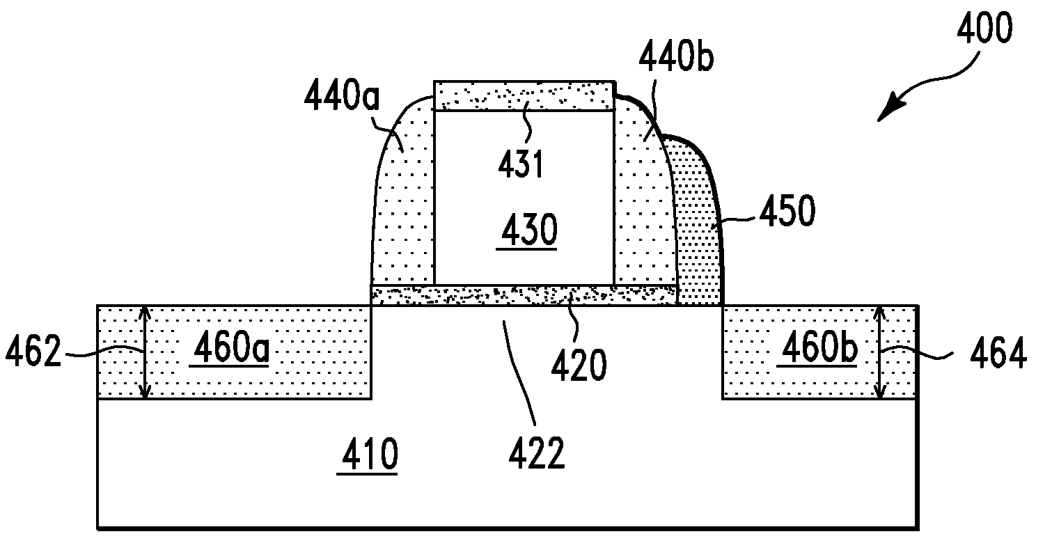
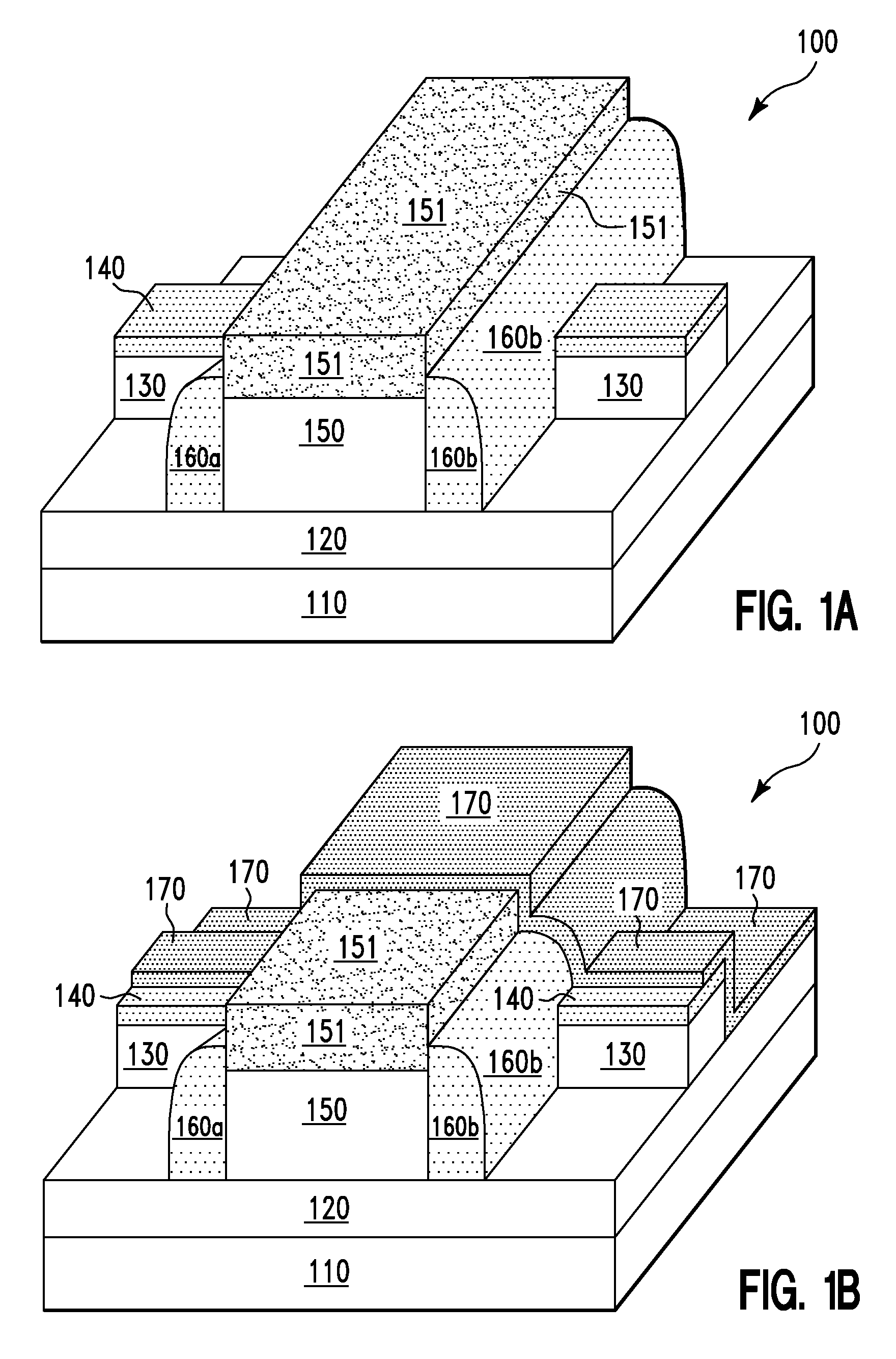
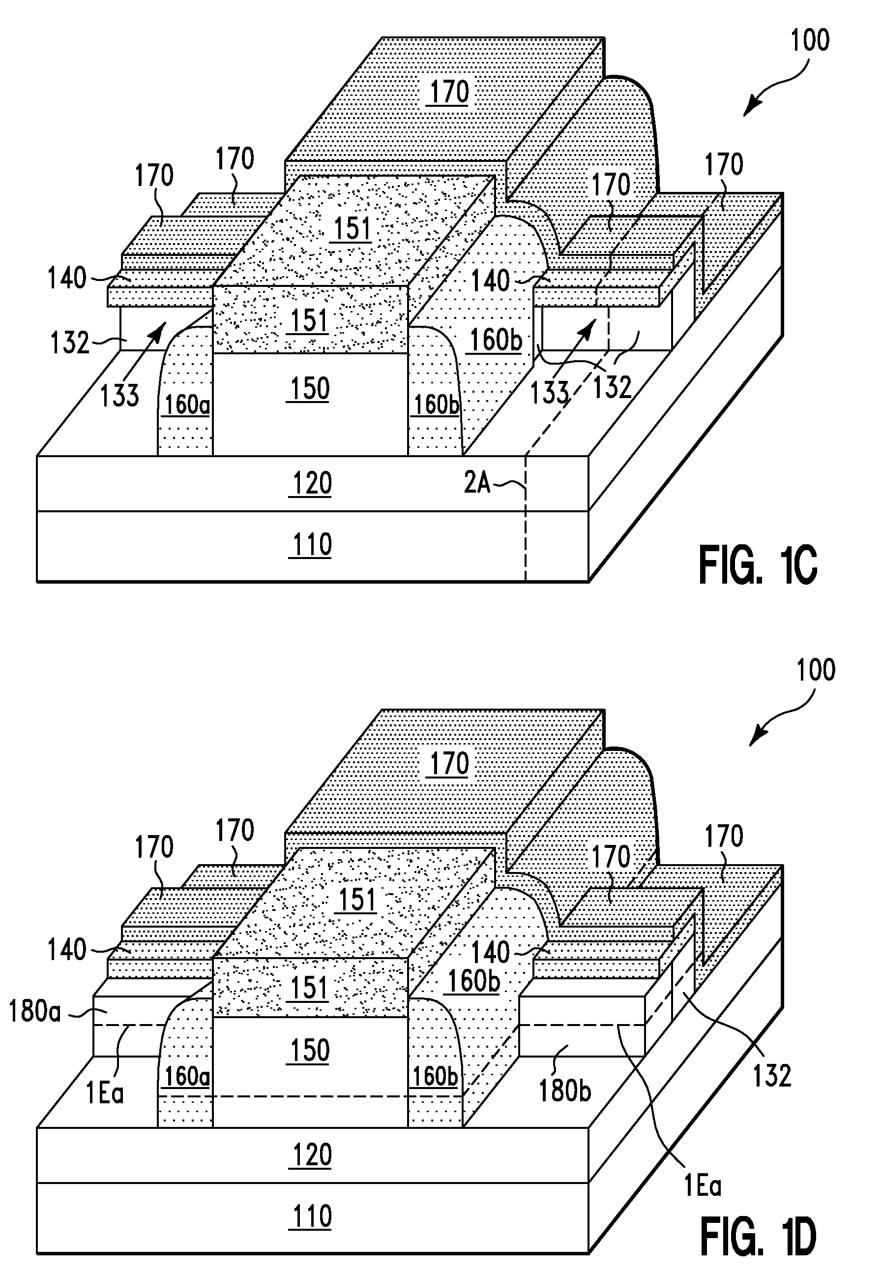
[0009]FIGS. 1A-1Eb (perspective views) illustrate a fabrication process for forming a vertical transistor (FinFET) structure 100, in accordance with embodiments of the present invention. More specifically, with reference to FIG. 1A, the fabrication of the vertical transistor structure 100 starts out with a structure including (i) a silicon (Si) substrate 110, (ii) a BOX (Buried Oxide) layer 120 on top of the Si substrate 110, (iii) a fin region 130 (comprising silicon in one embodiment) on top of the BOX layer 120, (iv) a hard mask 140 (comprising silicon nitride in one embodiment) on top of the fin region 130, (v) a gate electrode region 150 (comprising polysilicon in one embodiment) on top of the hard mask 140 and the BOX layer 120, (vi) a dielectric cap region 151 (comprising SiO2 in one embodiment) on top of the gate electrode region 150, and (vii) nitride spacers 160a and 160b (comprising silicon nitride in one embodiment) on side walls of the gate electrode region 150 and the ...


PUM


Abstract

A structure formation method. First, a structure is provided including (a) a fin region comprising (i) a first source/drain portion having a first surface and a third surface parallel to each other, not coplanar, and both exposed to a surrounding ambient, (ii) a second source/drain portion having a second surface and a fourth surface parallel to each other, not coplanar, and both exposed to the surrounding ambient, and (iii) a channel region disposed between the first and second source/drain portions, (b) a gate dielectric layer, and (c) a gate electrode region, wherein the gate dielectric layer (i) is sandwiched between, and (ii) electrically insulates the gate electrode region and the channel region. Next, a patterned covering layer is used to cover the first and second surfaces but not the third and fourth surfaces. Then, the first and second source/drain portions are etched at the third and fourth surfaces, respectively.

Description

FIELD OF THE INVENTION[0001]The present invention relates to transistors, having asymmetrically strained source / drain portions.BACKGROUND OF THE INVENTION[0002]In a conventional transistor, source / drain regions are usually etched, and then SiGe (silicon-germanium) or SiC (silicon-carbon) is epitaxially grown on source / drain portions of the fin region to provide strain into a channel region of the FET. However, the resulting structure usually does not have the optimum strain in the channel region. Therefore, there is a need for a method of forming a transistor that provides strain in the channel region higher than that of prior art.SUMMARY OF THE INVENTION[0003]The present invention provides a structure fabrication method. The method comprises providing a structure which includes (a) a fin region comprising a first semiconductor material, wherein the fin region includes (i) a first source / drain portion having a first surface and a third surface, wherein the first and third surfaces a...

Claims


Application Information

Patent Timeline
IPC IPC(8): H01L21/336
CPCH01L29/66795H01L29/785H01L29/7848
Inventor ANDERSON, BRENT ALANBRYANT, ANDRESNOWAK, EDWARD JOSEPH
Owner GLOBALFOUNDRIES INC
Why Eureka
Try Eureka