Susceptor, semiconductor manufacturing apparatus, and semiconductor manufacturing method

a manufacturing apparatus and semiconductor technology, applied in the direction of chemically reactive gases, coatings, crystal growth processes, etc., can solve the problems of inability to stably hold the wafer, the wafer is disadvantageously contaminated, and the wafer cannot be easily blocked from being contaminated, so as to improve productivity and minimize the fluctuation of the film thickness

Active Publication Date: 2009-11-05
NUFLARE TECH INC
View PDF9 Cites 22 Cited by
  • Summary
  • Abstract
  • Description
  • Claims
  • Application Information

AI Technical Summary

Benefits of technology

[0014]An embodiment of the present invention provides a semiconductor manufacturing apparatus and a semiconductor manufacturing method which use a susceptor configuration a temperature of which can be controlled and minimize a fluctuation in film thickness of a formed film to improve productivity.

Problems solved by technology

Therefore, the wafer is disadvantageously contaminated by diffusion and movement of metal atoms.
Therefore, the wafer cannot be easily blocked from being contaminated, in particular, through the pin hole.
Therefore, the wafer cannot be stably held.
Furthermore, when film formation is performed by heating and rotating the wafer and supplying a process gas, uniform film formation is difficult in such an unstable state.
In order to perform uniform film formation, the wafer may deviate from a susceptor placing position in high-speed rotation, and uniform film formation by the high-speed rotation is disadvantageously difficult.
As described above, when the susceptor structure which is free from a pin hole is employed to block the wafer from being contaminated through a pin hole formed in the susceptor, it is disadvantageously difficult that uniform film formation is performed while stably holding the wafer.

Method used


Image

  • Susceptor, semiconductor manufacturing apparatus, and semiconductor manufacturing method
  • Susceptor, semiconductor manufacturing apparatus, and semiconductor manufacturing method
  • Susceptor, semiconductor manufacturing apparatus, and semiconductor manufacturing method

Examples


embodiment 1

[0027]An embodiment of the present invention will be described below with reference to the accompanying drawings.

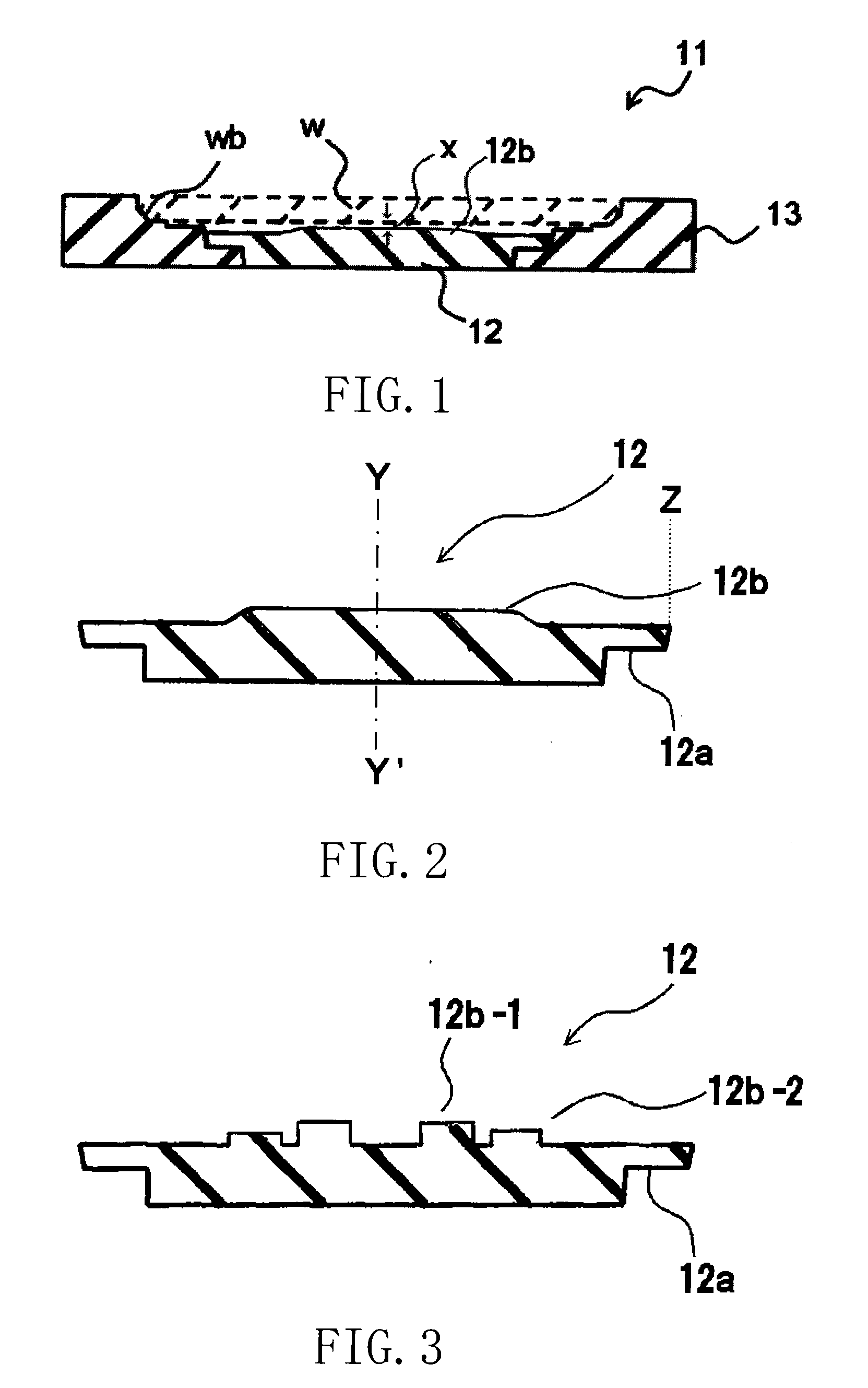
[0028]FIG. 1 shows a sectional view of a susceptor according to the embodiment. As shown in FIG. 1, a susceptor 11 includes an inner susceptor 12 and an outer susceptor 13 which can be separated from the inner susceptor 12.

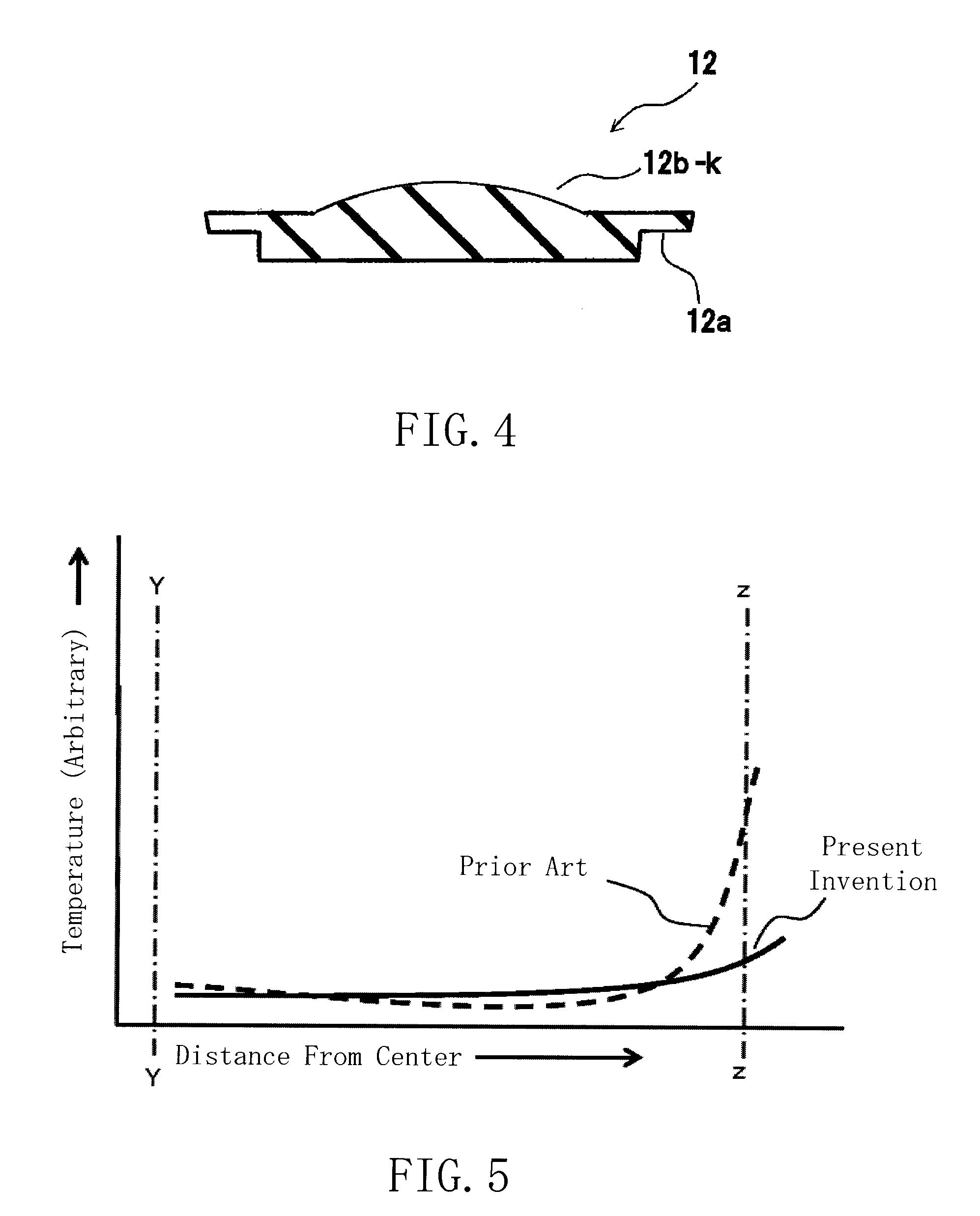
[0029]On the inner susceptor 12, as shown in FIG. 2, a step portion 12a is formed on an edge portion to have a size smaller than a diameter of a wafer w to be placed. On an upper surface of the step portion 12a, a disk-like convex portion 12b having, for example, a planar top surface is formed. The disk-like convex portion 12b is arranged to have a void (x) between a rear surface of the wafer w and the top surface (the top surface has a planar portion) of the convex portion 12b while the wafer w is placed. A size of the void (x) varies depending on a temperature distribution in a lateral direction of the wafer w. In FIG. 2, a center line serving as a ce...


PUM

PropertyMeasurementUnit
temperatureaaaaaaaaaa
sizeaaaaaaaaaa

Abstract

A susceptor includes a first step portion on which a wafer is placed; and a convex portion placed on a bottom surface of the first step portion, wherein a void is formed between a top surface of the convex portion and a rear surface of the wafer in a state in which the wafer is placed on the top surface of the convex portion.

Description

CROSS-REFERENCE TO RELATED APPLICATION[0001]This application is based upon and claims the benefit of priority from prior Japanese Patent Application No. 2008-120159 filed on May 2, 2008 in Japan, the entire contents of which are incorporated herein by reference.BACKGROUND OF THE INVENTION[0002]1. Field of the Invention[0003]The present invention relates to a susceptor, a semiconductor manufacturing apparatus, and a semiconductor manufacturing method which are used to supply a reaction gas to a front surface of, for example, a semiconductor wafer while heating the semiconductor wafer from a rear surface thereof to perform film formation and which are to hold the semiconductor wafer.[0004]2. Related Art[0005]In general, in a CVD (Chemical Vapor Deposition) apparatus used in formation of an epitaxial film in semiconductor manufacturing steps, a heat source and a rotating mechanism are arranged under a wafer, and a rear-surface heating method which can supply a uniform process gas from ...

Claims


Application Information

Patent Timeline
Patent Type & Authority Applications(United States)
IPC IPC(8): C23C16/458H01L21/46
CPCC23C16/4583C23C16/46H01L21/6875H01L21/68735C30B25/12H01L21/205
Inventor ITO, HIDEKI
Owner NUFLARE TECH INC
Why Eureka
Try Eureka