Manufacturing method of thin-film transistor, thin-film transistor sheet, and electric circuit

a manufacturing method and technology of thin-film transistors, applied in the direction of transistors, solid-state devices, semiconductor devices, etc., can solve the problems of large-scale display panels, poor channel accuracy, and large increase in manufacturing costs or running costs, so as to facilitate and efficiently manufacture, the effect of minimizing the fluctuation of their performance and high accuracy

Inactive Publication Date: 2008-05-06
FLEX DISPLAY SOLUTIONS LLC
View PDF17 Cites 22 Cited by
  • Summary
  • Abstract
  • Description
  • Claims
  • Application Information

AI Technical Summary

Benefits of technology

[0008]The present invention has been made in view of the above. An object of the invention is to provide a method of easily and efficiently manufacturing a thin-film transistor, a thin-film transistor sheet and an electric circuit, each having high accuracy, without employing a vacuum system process requiring a large scale manufacturing facility. Another object of the invention is to provide a method of stably manufacturing a thin-film transistor a thin-film transistor sheet and an electric circuit, minimizing fluctuation of their performance.

Problems solved by technology

In the manufacture of a flat panel display employing such a TFT, a photolithography step with high precision is required in addition to a thin layer forming step requiring a vacuum line carrying out a CVD method or a sputtering method or a high temperature treatment step, which results in great increase of manufacturing cost or running cost.
Recent demand for a large-sized display panel further increases those costs described above.
These methods have problem in that the channel accuracy are poor, resulting in fluctuation of its performance of the resulting thin-film transistor.
Further, as the methods described above have problem in that as SD electrodes are formed employing a liquid material, the electrodes are likely to be short-circuited which may make it impossible to manufacture a thin-film transistor.

Method used


Image

  • Manufacturing method of thin-film transistor, thin-film transistor sheet, and electric circuit
  • Manufacturing method of thin-film transistor, thin-film transistor sheet, and electric circuit
  • Manufacturing method of thin-film transistor, thin-film transistor sheet, and electric circuit

Examples


example 1

>Bottom Gate Type

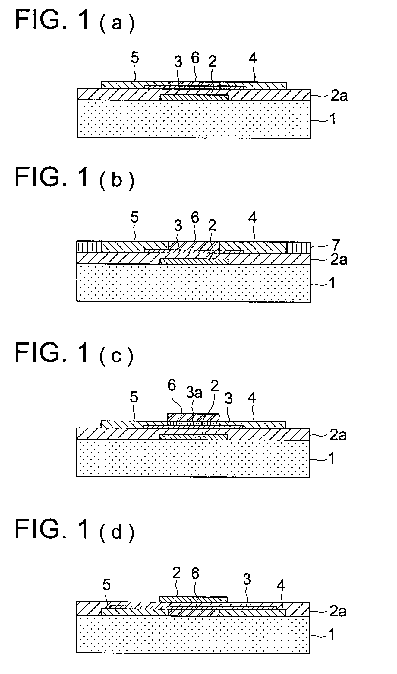
[0288]A thin-film transistor sample 1, having a layer structure as shown in FIG. 1(a), was prepared according to the following procedures.

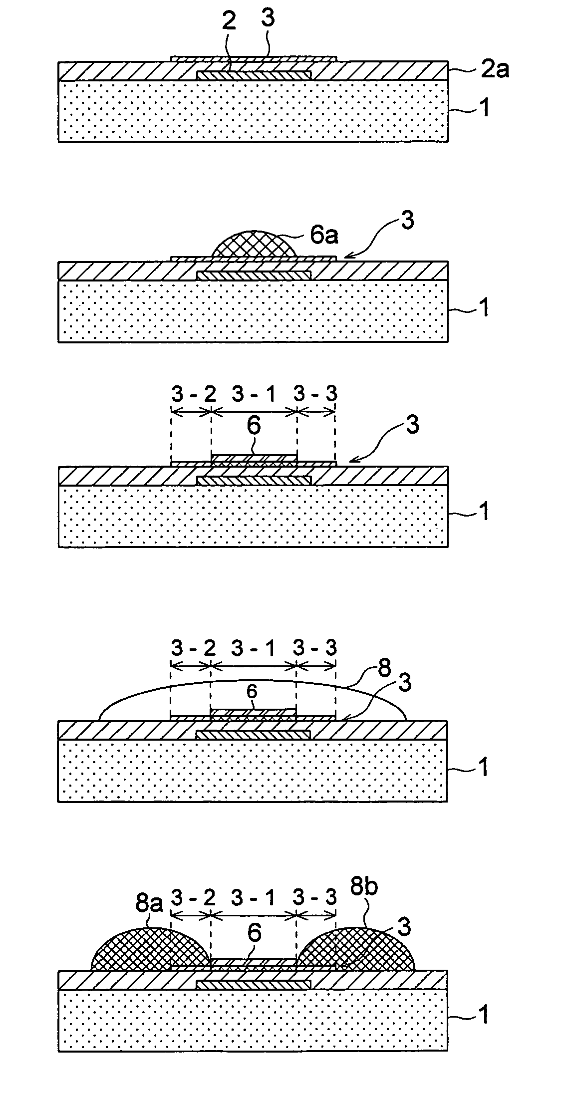
[0289]In the procedures, procedures 1 through 3 will be explained employing FIG. 3(1) through 3(6). FIG. 1(a) has the same structure as FIG. 3(6).

Procedure 1: FIG. 3(1) Gate electrode 2, gate insulating layer 2a, and organic semiconductor layer 3 were provided on a substrate 1 as follows to obtain a layer structure as shown in FIG. 3(1).

[0290]The surface of substrate 1 of a 200 μm thick PES film was corona discharged at 50 W / m2 / min and then coated with a coating liquid having the following composition to obtain a layer of a dry thickness of 2 μm. The resulting layer was dried at 50° C. for 5 minutes, and hardened by being exposed for 4 seconds employing a 60 W / cm high pressure mercury lamp 10 cm distant from the layer.

[0291]

Dipentaerythritol hexacrylate monomer60 gDipentaerythritol hexacrylate dimmer20 gDipentaerythritol hexacryla...

example 2

[0314]Thin-film transistor sample 2 was prepared in the same manner as in thin-film transistor sample 1 of Example 1, except that the insulating area 6 was formed employing a composition, which was obtained kneading a mixture of the silicone adhesive and carbon (content ratio 2:1 by weight), instead of the silicone adhesive. The thin-film transistor sample 2 was evaluated in the same manner as in Example 1.

[0315]The thin-film transistor sample 2 exhibited the same good working property as thin-film transistor sample 1. A white light transmittance of the insulating layer of this sample 2 was 0.1%, and when the sample was operated under a fluorescent lamp of 3000 Lux, its property did not vary.

example 3

[0316]Thin-film transistor sample 3 was prepared in the same manner as in thin-film transistor sample 1 of Example 1, except that an organic semiconductor layer, a source electrode and a drain electrode were formed as follows:

1. Formation of Organic Semiconductor Layer

[0317]A chloroform solution of regioregular poly(3-hexylthiophene), (produced by Ardrich Co., Ltd.), which had been purified to have a Zn and Ni content of not more than 10 ppm, was prepared. This solution was ejected employing a piezo type ink jet printer, dried at room temperature and heat treated at 50° C. for 30 minutes in a nitrogen atmosphere to form an organic semiconductor layer of poly(3-hexylthiophene) with a thickness of 30 nm.

2. Formation of Source Electrode and Drain Electrode

[0318]A silver paste Dotite D-550 (produced by Fujikura Kasei Co., Ltd.) was coated on the insulating area, and dried to form a source electrode and a drain electrode.

[0319]The thin-film transistor sample 3 exhibited good working prop...


PUM

PropertyMeasurementUnit
thicknessaaaaaaaaaa
thicknessaaaaaaaaaa
light transmittanceaaaaaaaaaa

Abstract

A thin-film transistor, a thin-film transistor sheet, an electric circuit, and a manufacturing method thereof are disclosed, the method comprising the steps of forming a semiconductor layer by providing a semiconductive material on a substrate, b) forming an isolating area, which is electrode material-repellent, by providing an electrode material-repellent material on the substrate, and c) forming a source electrode on one end of the insulating area and a drain electrode on the other end of the insulating area, by providing an electrode material.

Description

FIELD OF THE INVENTION[0001]The present invention relates to a method of a thin-film transistor, a thin-film transistor sheet, and an electric circuit.BACKGROUND OF THE INVENTION[0002]With the spread of information terminals, there are increasing demands for a flat panel display that serves as a display for a computer. Further, with development of the information technology, there has been increased a chance for information offered in a form of a sheet of paper medium in the past to be offered in an electronic form. An electronic paper or digital paper is demanded increasingly as a display medium for a mobile that is thin, lightweight and handy.[0003]In the case of a display device of a flat sheet type, a display medium is generally formed using an element that employs a liquid crystal, organic EL or electrophoresis method. In the display medium of this kind, a technology for using an active driving element comprised of a thin-film transistor (TFT), serving as an image driving eleme...

Claims


Application Information

Patent Timeline
Patent Type & Authority Patents(United States)
IPC IPC(8): H01L29/04H01L21/00H01L21/316H01L27/28H01L29/786H01L51/00H01L51/05H01L51/10H01L51/30H01L51/40
CPCH01L27/283H01L51/0021H01L51/0022H01L51/052H01L51/0541H01L51/0545H01L51/105H01L21/31683H01L21/31687H01L51/0037H01L51/0052H10K19/10H10K71/611H10K71/60H10K85/1135H10K85/615H10K10/471H10K10/464H10K10/466H10K10/84H01L21/02244
Inventor HIRAI, KATSURA
Owner FLEX DISPLAY SOLUTIONS LLC
Why Eureka
Try Eureka