
Sensing circuit, method of driving sensing circuit, display device, method of driving display device, and electronic apparatus

a sensing circuit and sensing circuit technology, applied in the field of sensing circuits, can solve the problems of detection errors, difficult to accurately detect the contact position of objects, and large area, and achieve the effect of accurate detecting contact and high accuracy

Active Publication Date: 2009-11-05
JAPAN DISPLAY WEST
View PDF2 Cites 32 Cited by
  • Summary
  • Abstract
  • Description
  • Claims
  • Application Information

AI Technical Summary

Benefits of technology

[0007]An advantage of some aspects of the invention is that it provides a technique capable of accurately detecting contact between an object and a display device and specifying a contact position therebetween with high accuracy.
[0008]According to a first aspect of the invention, a display device includes: a first substrate and a second substrate that face each other; electro-optical elements (for example, liquid crystal elements 50 shown in FIG. 1) that are interposed between the first substrate and the second substrate; light detecting units that are provided between the first substrate and the second substrate and output first detection signals having levels corresponding to the amount of incident light; and capacitance detecting units that include capacitive elements (for example, capacitive elements C shown in FIG. 2, and capacitive elements C2 shown in FIG. 4) each having a first electrode (for example, an electrode 121 shown in FIGS. 2 to 4) and a second electrode (for example, an opposite electrode 55 shown in FIGS. 2 to 4) provided between the first substrate and the second substrate, output second detection signals having levels corresponding to the capacitance values of the capacitive elements, and are provided separately from the light detecting units. According to the display device of the first aspect, it is possible to accurately detect the contact between an object and the display device.
[0009]In the display device according to the first aspect, each of the capacitive elements may include the first electrode (for example, the electrode 121 shown in FIG. 2) provided on a surface of the first substrate facing the second substrate, the second electrode (for example, the opposite electrode 55 shown in FIG. 2) provided on a surface of the second substrate facing the first substrate, and an electro-optical material (for example, liquid crystal 57 shown in FIG. 2) interposed between the first electrode and the second electrode. Each of the second electrodes may be provided on the surface of the second substrate facing the first substrate so as to cover a first protruding portion (for example, a protruding portion 140b shown in FIG. 2) that protrudes toward the first substrate. According to this structure, since the second electrode is provided on the surface of the second substrate facing the first substrate so as to cover the first protruding portion that protrudes toward the first substrate, it is possible to reduce the gap between the first electrode and the second electrode, as compared to a structure in which the first protruding portion is not provided. Therefore, it is possible to increase the capacitance value of the capacitive element. As a result, it is possible to detect a variation in the capacitance value of the capacitive element with high sensitivity.

Problems solved by technology

As a result, an excessively large area is likely to be specified as the contact position between the object and the display device.
That is, it is difficult to accurately detect the contact position of the object.
As a result, it may be determined that the object contacts the screen, which is a detection error.
Therefore, it is difficult to accurately determine whether the object contacts or approaches the screen.
That is, there is a concern that the contact position of the object will be erroneously specified.

Method used


Image

  • Sensing circuit, method of driving sensing circuit, display device, method of driving display device, and electronic apparatus
  • Sensing circuit, method of driving sensing circuit, display device, method of driving display device, and electronic apparatus
  • Sensing circuit, method of driving sensing circuit, display device, method of driving display device, and electronic apparatus

Examples


first embodiment

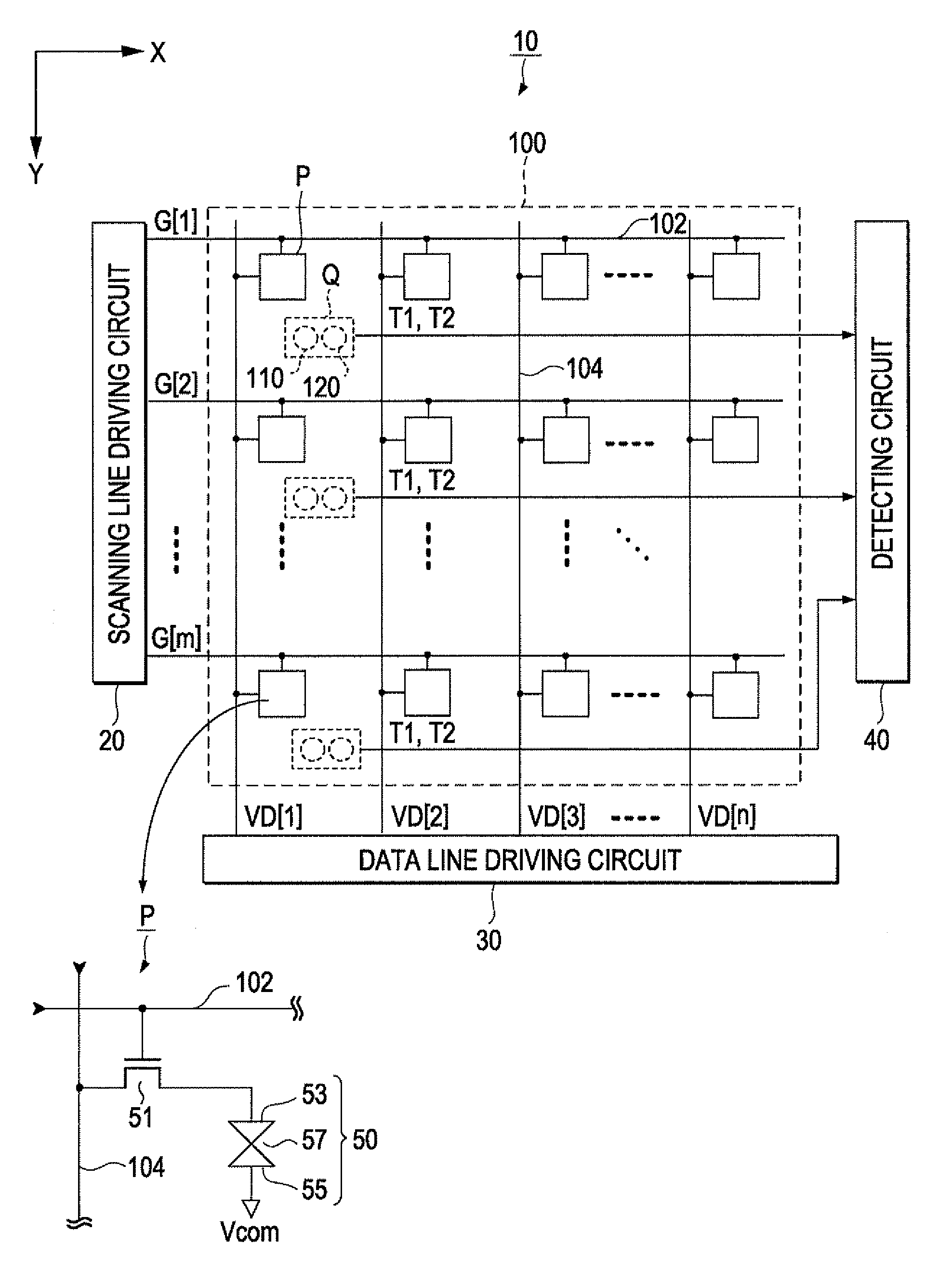
[0053]FIG. 1 is a block diagram illustrating the structure of a display device 10 according to a first embodiment of the invention. The display device 10 includes a pixel region 100 in which a plurality of pixel circuits P are arranged in a matrix, a scanning line driving circuit 20 and a data line driving circuit 30 that drive each of the pixel circuits P, and a detecting circuit 40 that detects the contact between an object and the display device 10. As shown in FIG. 1, the pixel region 100 includes m scanning lines 102 that extend in an X direction and n data lines 104 that extend in a Y direction orthogonal to the X direction (m and n are natural numbers that are equal to or greater than 2). The pixel circuits P are arranged at positions corresponding to intersections of the scanning lines 102 and the data lines 104. Therefore, the pixel circuits P are arranged in a matrix of m rows by n columns. In addition, a backlight (not shown) is provided on the rear side of the pixel regi...

second embodiment

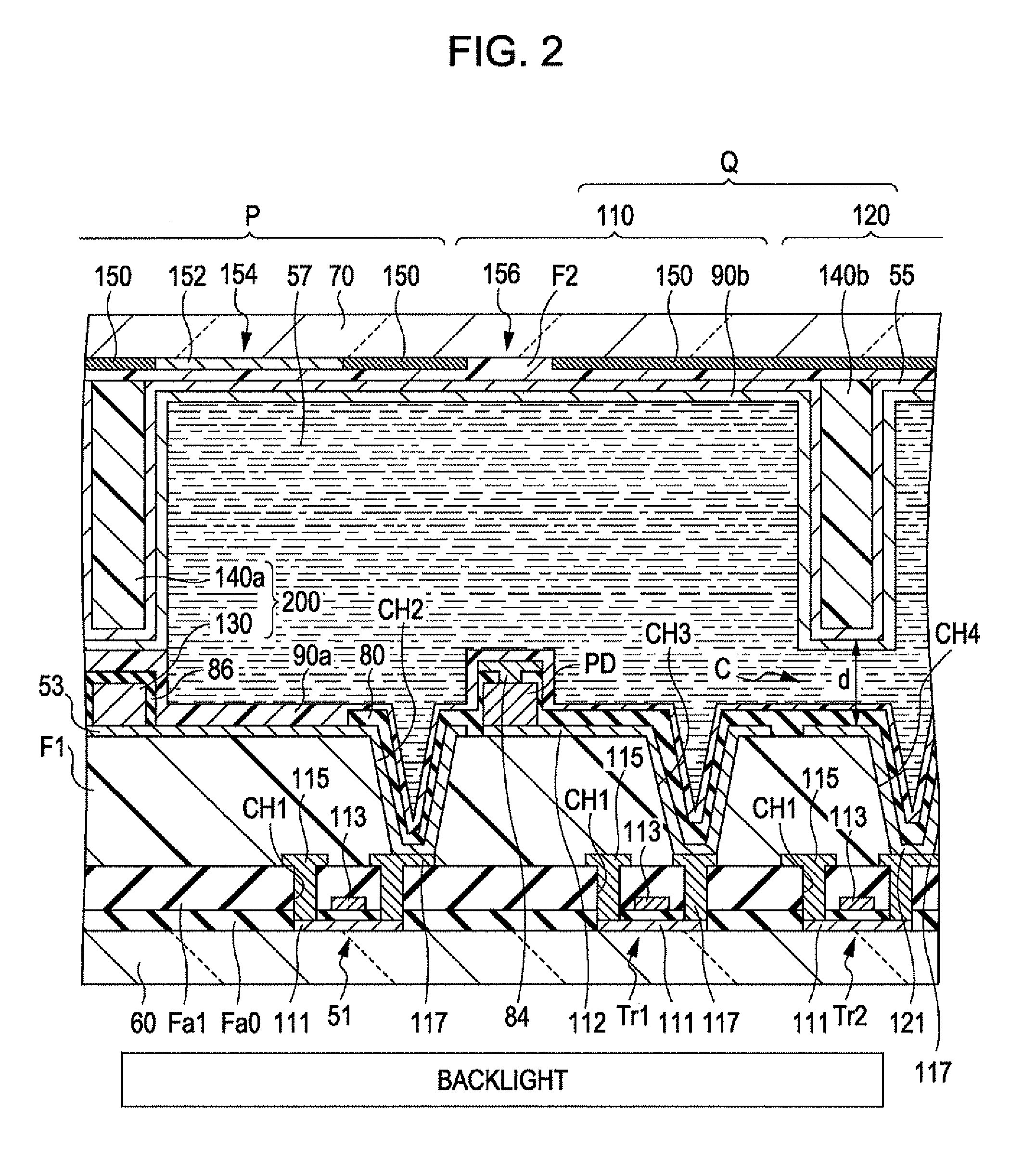
[0075]FIG. 3 is a cross-sectional view illustrating a display device 10 according to a second embodiment of the invention (which corresponds to the cross-sectional view of FIG. 1). In this embodiment, the dummy photodiode 130 is not provided, and a protruding portion 140c that protrudes toward the first substrate 60 is provided in a region corresponding to the photodiode PD (a region corresponding to the transmission hole 156) on a surface of the second planarizing layer F2 facing the first substrate 60. As shown in FIG. 3, the top surface of the photodiode PD (one end of the photodiode PD that protrudes toward the second substrate 70) and the top surface of the protruding portion 140c (one end of the protruding portion 140c that protrudes toward the first substrate 60) are contacted with each other by, for example, the alignment films 90a and 90b. That is, in this embodiment, a spacer 201 defining the gap between the first substrate 60 and the second substrate 70 includes the photo...

second modification

(2) Second Modification

[0084]In the above-described first embodiment, the spacer 200 includes the dummy photodiode 130 and the protruding portion 140a. However, for example, instead of the dummy photodiode 130, a protruding portion may be provided on the surface of the pixel electrode 53. For example, the spacer 200 may include the protruding portion 140a and a protruding portion (for example, the dummy photodiode 130) that is provided at a position that faces the protruding portion 140a on the surface of the second substrate 70 facing the first substrate 60 so as to protrude toward the first substrate 60.


PUM


Abstract

A display device includes: a first substrate and a second substrate that face each other; electro-optical elements that are interposed between the first substrate and the second substrate; light detecting units that are provided between the first substrate and the second substrate and output first detection signals having levels corresponding to the amount of incident light; and capacitance detecting units that include capacitive elements each having a first electrode and a second electrode provided between the first substrate and the second substrate, output second detection signals having levels corresponding to the capacitance values of the capacitive elements, and are provided separately from the light detecting units.

Description

BACKGROUND[0001]1. Technical Field[0002]The present invention relates to a technique for detecting contact.[0003]2. Related Art[0004]Display devices having a function of detecting the contact between an object, such as a finger or a pen, and a screen have been known. For example, JP-A-2007-47851, JP-A-2006-40289, and JP-A-2006-189868 disclose a first technique that detects a variation in the capacitance of a capacitive element including two electrodes opposite to each other and an electro-optical material, such as liquid crystal, interposed between the two electrodes to detect the contact between an object and a screen. In addition, for example, JP-A-2005-72126, JP-A-2004-119494, and JP-A-2008-27292 disclose a second technique that detects a variation in the amount of light incident on an optical sensor to detect the contact between an object and a screen.[0005]In the first technique, capacitance detecting units each including the capacitive element including two electrodes opposite...

Claims


Application Information

Patent Timeline
IPC IPC(8): G06F3/041
CPCG02F1/13338G06F3/044G06F3/042G06F3/0412G06F3/0446G06F3/0445
Inventor OTA, HITOSHIKANDA, EIJI
Owner JAPAN DISPLAY WEST
Learn More