Method and apparatus for probe contacting

Inactive Publication Date: 2011-06-09
HITACHI HIGH-TECH CORP
View PDF8 Cites 1 Cited by
  • Summary
  • Abstract
  • Description
  • Claims
  • Application Information

AI Technical Summary

Benefits of technology

[0024]According to this invention, there can be provided a method and device for acc

Problems solved by technology

Thus, the electrical method described in the Patent Document 1 cannot be used in this case.
However, in this method, there is a problem that the device is complicated.
Thus, there is a defect that it is not available until the distance between the mechanical probe and the sample to be processed becomes several μm.
In this method, since an AC voltage source is required to be provided, there is a problem that the device is complicated and increased in size.
In this method, since the two or more microscopes are required to be provided, there is a problem that the device is increased in size.
This method simply utilizes the reduction in brightness around the mechanical probe, and there is a problem that the reliability of the detection of the contact is low.
Accordingly, there is a problem that the device configuration is complicated.
As described above, in the method of detecting the contact of

Method used


Image

  • Method and apparatus for probe contacting
  • Method and apparatus for probe contacting
  • Method and apparatus for probe contacting

Examples


Embodiment Construction

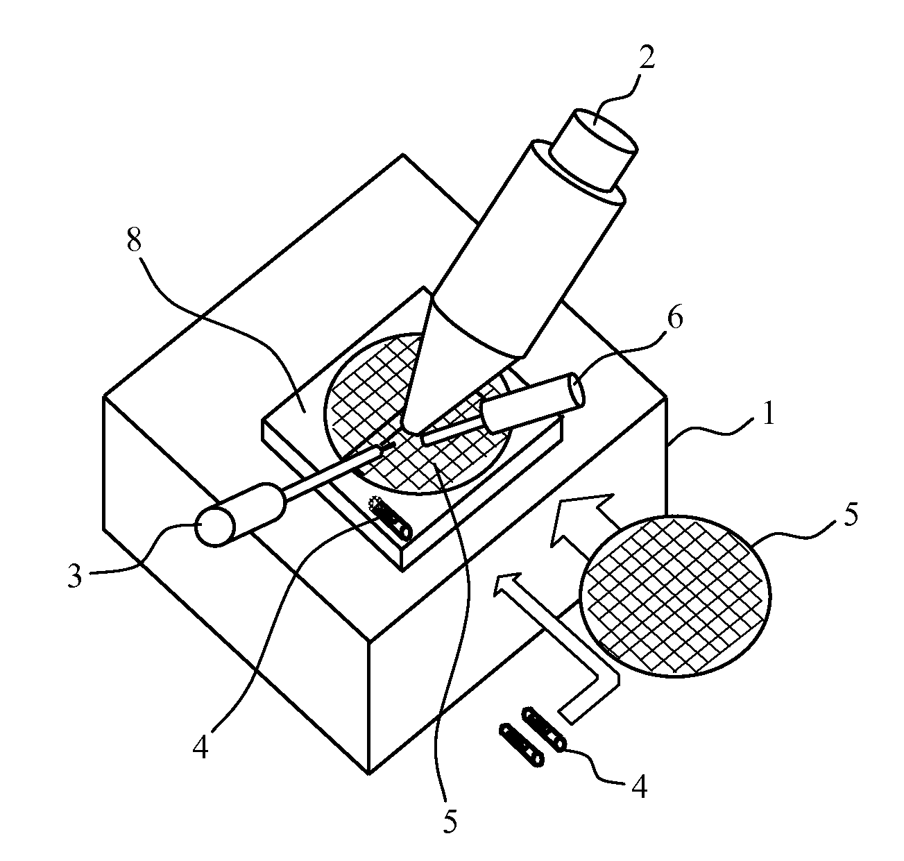
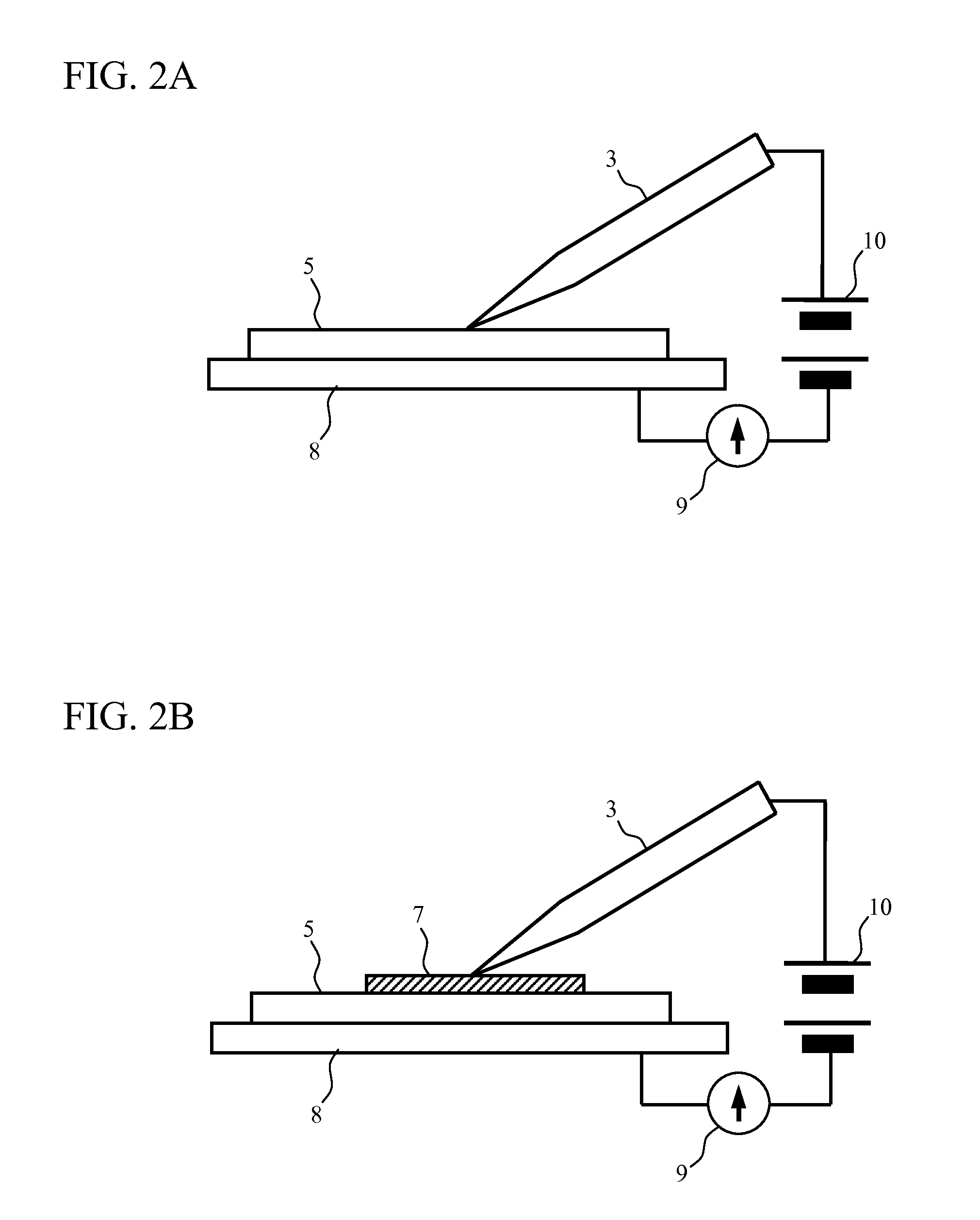
[0053]The outline of a focused ion beam system or a charged particle beam system according to this invention will be described with reference to FIG. 1. The focused ion beam system of this example has a focused ion beam source 2 generating a focused ion beam, a sample table 8 supporting a sample 5, a mechanical probe 3 used in the operation of cutting out a minute sample piece from the sample 5, a conveying holder 4 holding the minute sample piece cut out from the sample 5, and a gas assisted gun (a deposition gun or a deposition / etching gun) 6 used in a deposition operation. Those components are provided in a sample chamber 1.

[0054]An outline of the processing of cutting out the minute sample piece from the sample 5 by the focused ion beam system of this example will be described. First, the sample 5 and the conveying holder 4 are arranged on the sample table 8. In this example, although the sample 5 is described as a semiconductor wafer, the sample 5 may be any object. Next, the m...


PUM


Abstract

There is provided a method and a device for accurately detecting the contact of a mechanical probe with a contact object. The contact detecting device comprises a mechanical probe movable for being in contact with a contacted object, a charged particle beam source which generates a charged particle beam applied to the contacted object, a detector for detecting secondary particles or reflected particles from the contacted object, a calculating device which calculates, from a detection signal from the detector, a feature quantity of a shadow of the mechanical probe projected on the contacted object, and a control device which controls the operation of the mechanical probe. The calculating device calculates, as the feature quantity of the shadow of the mechanical probe, a shadow depth S(x, y), and obtains an evaluation value J(z), showing a distance between the contacted object and the mechanical probe, based on the shadow depth S(x, y).

Description

TECHNICAL FIELD[0001]This invention relates to a processing apparatus and an inspection apparatus for a semiconductor device.BACKGROUND ART[0002]Recently, with miniaturization and higher functionality of a semiconductor device, a cross section structure of the semiconductor device is required to be observed and inspected in addition to inspection of the surface pattern of the semiconductor device. In the inspection of the structure of the semiconductor device, a minute sample piece is cut out from the semiconductor device to be observed by an electron microscope. In order to cut out the minute sample piece from the semiconductor device, a charged particle beam system including a mechanical probe and a deposition gun or a focused ion beam system is used.[0003]In the above processing apparatus, when the minute sample piece is cut out, the mechanical probe should be in contact with the surface of the sample. Accordingly, the processing apparatus is provided with a device for detecting ...

Claims


Application Information

Patent Timeline
IPC IPC(8): G01R31/20
CPCG01R31/2891H01J37/28H01J2237/2482H01J2237/24592H01J2237/208
Inventor MORITA, KAZUHIROUMEMURA, KAORU
Owner HITACHI HIGH-TECH CORP
Why Eureka
Try Eureka