

Method and apparatus for generating adaptive noise and timing models for VLSI signal integrity analysis
a signal integrity analysis and adaptive noise technology, applied in the field of computer operations and applications, can solve the problems of insufficient processing time for the needed simulation of large vlsi designs, inability to perform the required simulations in large circuits, and inability to speed up the search process, so as to achieve the effect of speeding up the search process
- Summary
- Abstract
- Description
- Claims
- Application Information
AI Technical Summary
Benefits of technology
Problems solved by technology
Method used
Image

Examples
Embodiment Construction
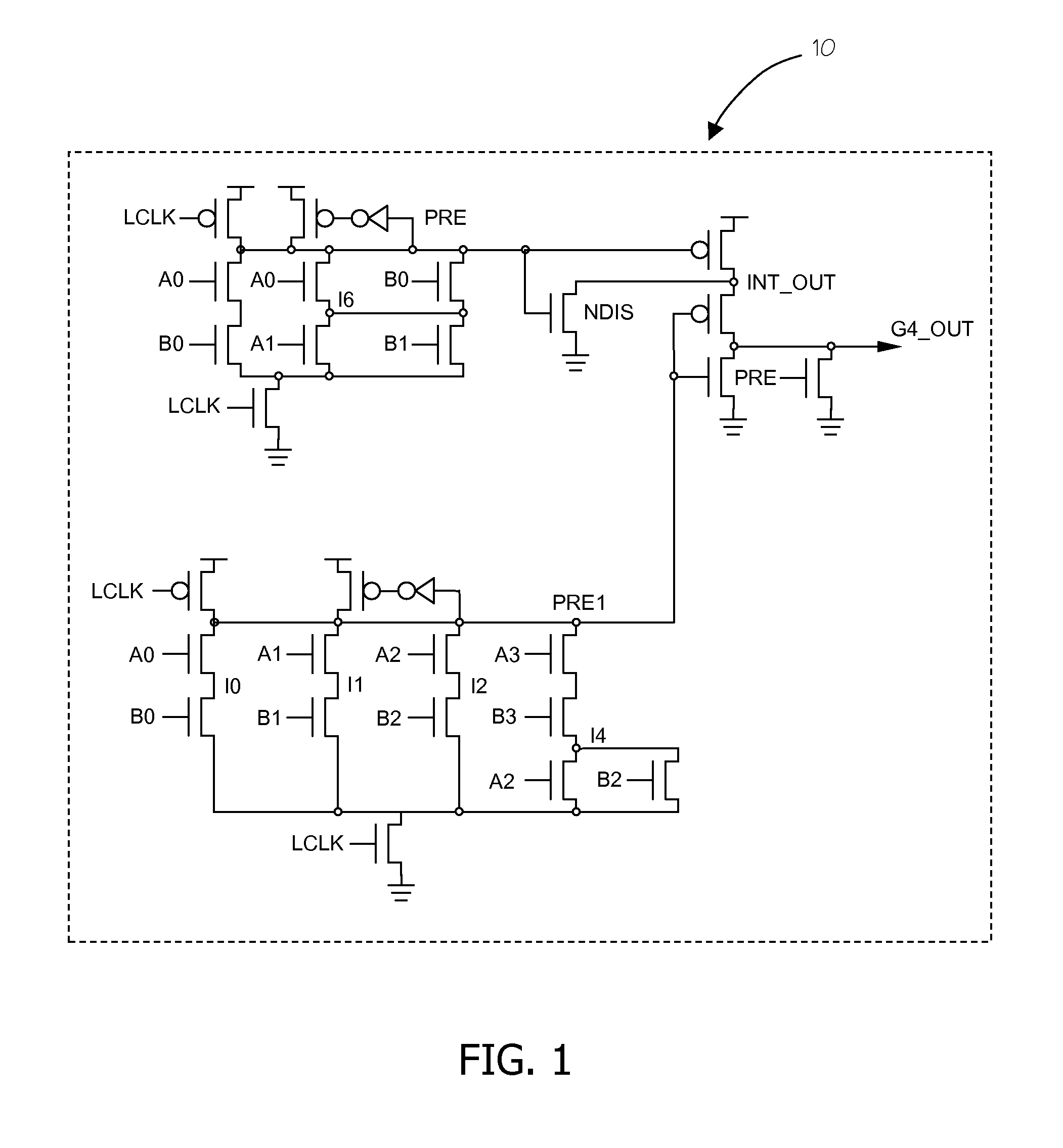
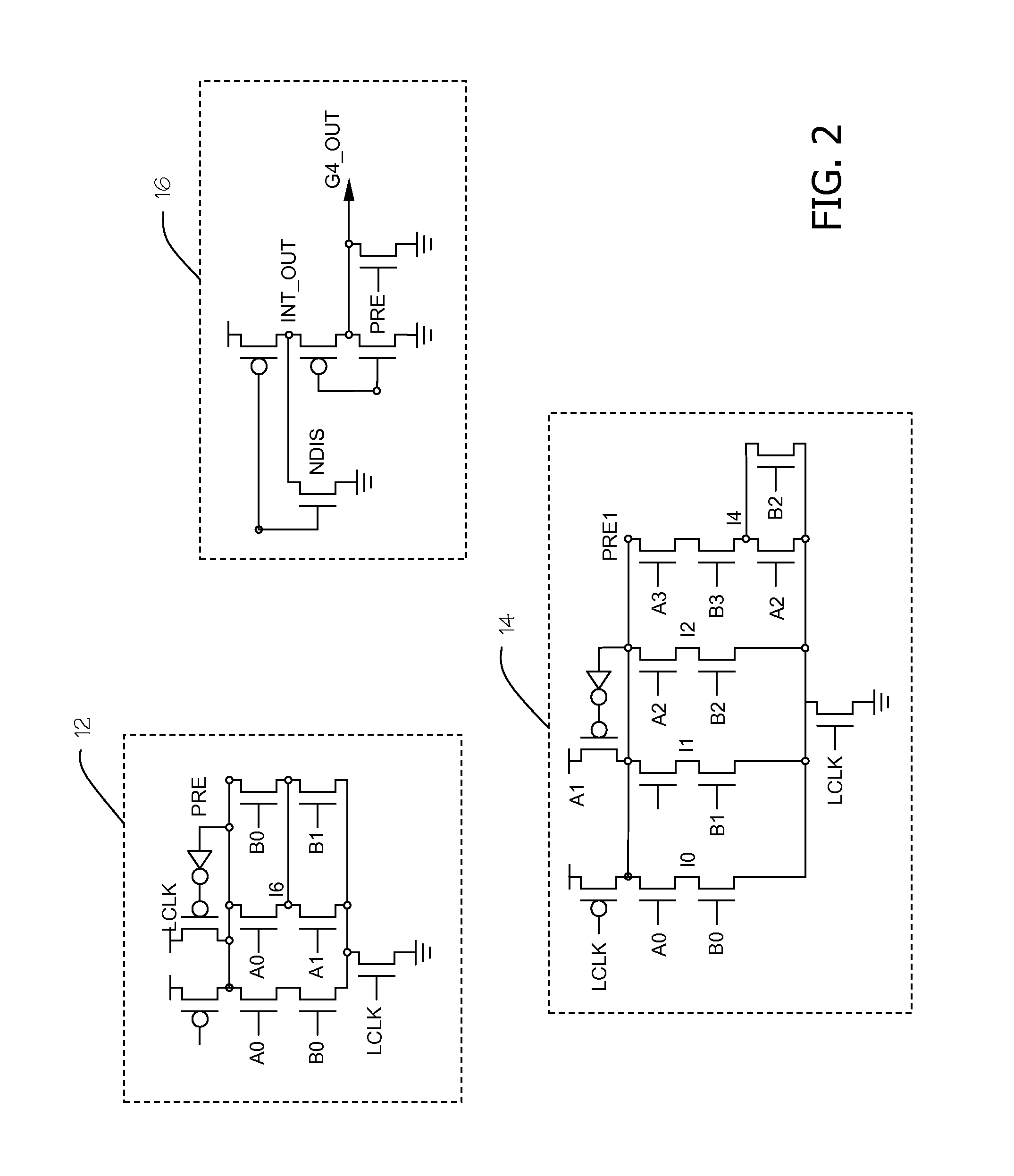
[0018]A contemporary method to perform signal integrity analysis on large designs is to break the designs into individual gates or sub-circuits. The larger design is broken into smaller portions or sub-circuits generally where devices are connected through their source / drain nodes. Analysis may then be performed on these sub-circuits with their results being combined to provide results for the entire macro. For example, FIG. 1 shows an exemplary macro 10 containing typical elements. The macro in FIG. 1 could be broken into sub-circuits 12, 14 and 16 as illustrated in FIG. 2. One method for decomposing the macro into sub-circuits is disclosed in U.S. Pat. No. 6,601,220, which is incorporated by reference herein in its entirety.
[0019]Methods for decomposing the sub-circuits into channel connected components are well known to those skilled in the art. Briefly, they involve grouping non-intersecting transistors that are connected by source and drain terminals to each other, and to suppl...
PUM
 Abstract
Description
Claims
Application Information