Solder ball mounting apparatus and wiring board manufacturing method

a technology of soldering apparatus and wiring board, which is applied in the direction of soldering apparatus, non-printed mask, and semiconductor/solid-state device details, etc., to achieve the effect of reducing connection failures and suppressing defects

Inactive Publication Date: 2009-11-19
NGK SPARK PLUG CO LTD
View PDF3 Cites 15 Cited by
  • Summary
  • Abstract
  • Description
  • Claims
  • Application Information

AI Technical Summary

Benefits of technology

[0007]The present invention was made in consideration of the above circumstances, and an object thereof is to provide a solder ball mounting apparatus capable of suppressing defects caused by solder balls that have fallen out of or otherwise been dislocated from a wiring board and a method for manufacturing a wiring board capable of reducing the connection failures caused by the missing or out of place solder balls.

Problems solved by technology

Despite the existence of such problems, the above-described patent documents do not provide a solution for sufficiently overcoming the dislocation of solder balls from the electrodes during the wiring board manufacturing process.

Method used


Image

  • Solder ball mounting apparatus and wiring board manufacturing method
  • Solder ball mounting apparatus and wiring board manufacturing method
  • Solder ball mounting apparatus and wiring board manufacturing method

Examples


modification 1

[0065]B1. Modification 1

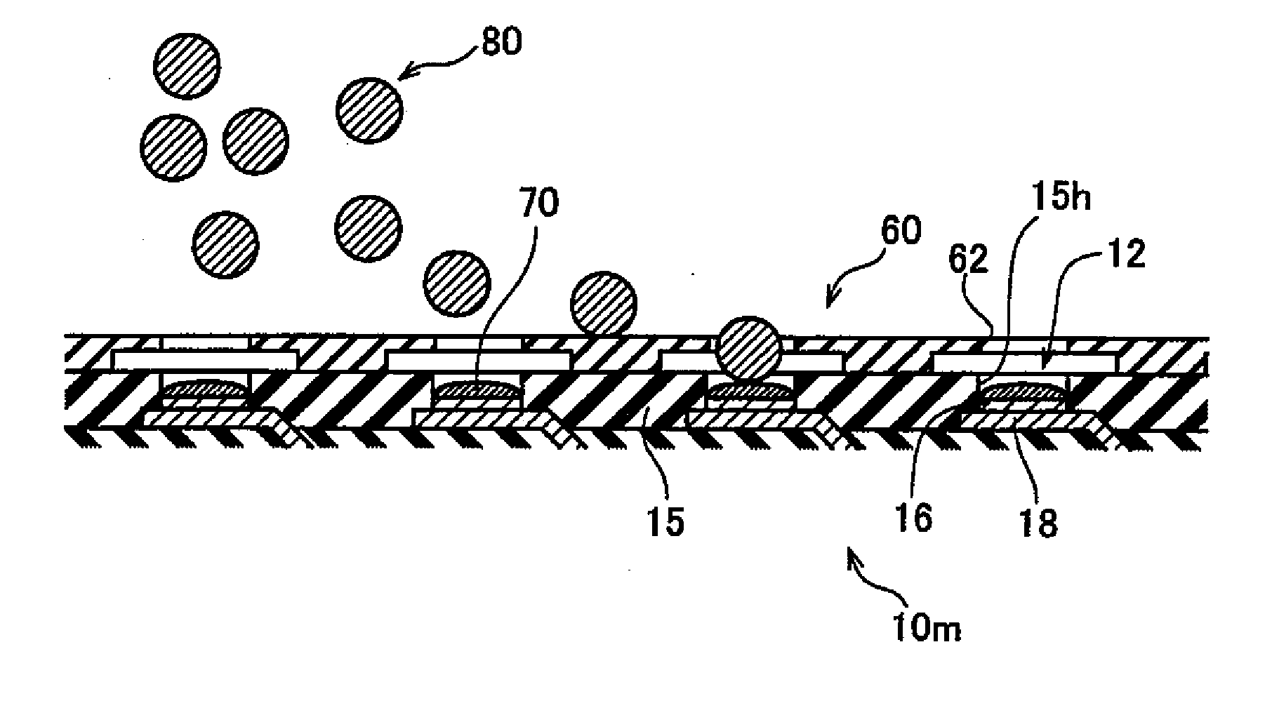
[0066]In the solder ball removing unit 100 in the exemplary embodiment, although the solder ball removing portion 110 sweeps out the extra solder balls 82 by the removing brushes 115 which are driven to rotate, the extra solder balls 82 may be removed by other methods. For example, the solder ball removing portion 110 may blow out the extra solder balls 82 by air jetted under high pressure.

[0067]In the solder ball removing unit 100 in the exemplary embodiment, the solder ball pressing portion 120 presses the regularly disposed solder balls 81 towards the electrodes 16 by pressing the pressing brush 123 by the brush pressing portion 124. However, the solder ball pressing portion 120 may press the regularly disposed solder balls 81 towards the electrodes 16 by other methods. For example, the brush pressing portion 124 may be omitted, and the pressing brush 123 may be urged by a spring mechanism so as to press the regularly disposed solder balls 81. In addition,...

modification 2

[0068]B2. Modification 2

[0069]In the solder ball removing unit 100 in the exemplary embodiment, the solder ball removing portion 110 and the solder ball pressing portion 120 are unified, and the extra solder ball 82 removing step and the regularly disposed solder ball 81 pressing step are executed simultaneously (i.e., in parallel). However, the solder ball removing portion 110 and the solder ball pressing portion 120 may be separate from each other. In other words, the extra solder ball 82 removing step by the solder ball removing portion 110 may be implemented first, and thereafter, the regularly disposed solder ball 81 pressing step may be implemented by the solder ball pressing portion 120.

modification 3

[0070]B3. Modification 3

[0071]In the exemplary embodiment described above, the brushes 115, 123 are formed of the conductive members but may be formed of a non-conductive member. However, when the brushes 115, 123 are formed of the conductive member, since the generation of static electricity is decreased, it becomes possible to decrease the dislocation of the regularly disposed solder balls 81 from the disposed positions caused by the regularly disposed solder balls 81 being attracted by static electricity.


PUM

PropertyMeasurementUnit
diameteraaaaaaaaaa
diameteraaaaaaaaaa
conductiveaaaaaaaaaa

Abstract

A wiring board includes an insulating layer having a plurality of through holes formed therein, a base substrate layer positioned below the insulating layer, and a plurality of electrodes disposed on the base substrate layer, each electrode having an exposed surface exposed from a respective through hole, each exposed surfaces being coated with a flux. A plurality of solder balls are disposed on the fluxes in the through holes, respectively. An apparatus for mounting the solder balls on the plurality of electrodes includes: a solder ball removing unit configured to remove a first plurality of solder balls located other than in the through holes; and a solder ball pressing unit configured to press a second plurality of solder balls individually disposed in the through holes towards respective electrodes and into respective flux.

Description

CROSS-REFERENCE TO RELATED APPLICATIONS[0001]This application is based on and claims priority to Japanese patent Application No. 2008-123346 filed May 9, 2008, the above application incorporated herein by reference in its entirety.BACKGROUND OF THE INVENTION[0002]1. Field of the Invention[0003]The present invention relates to a solder ball mounting apparatus for mounting solder balls on a wiring board and a method for manufacturing a wiring board in which solder bumps are formed on electrodes.[0004]2. Description of Related Art[0005]A wiring board for mounting electronic components, such as LSI or IC chips, generally includes an insulating layer provided on an outer surface of a base substrate having a wiring pattern of the wiring board. Some types of wiring boards include solder bumps formed on outer surfaces of electrodes (pads) which are exposed from the insulating layer. Solder bumps are formed by disposing solder balls on a flux coated on surfaces of electrodes on the wiring bo...

Claims


Application Information

Patent Timeline
Patent Type & Authority Applications(United States)
IPC IPC(8): B23K1/20B23K3/06
CPCH05K3/3478H05K2203/0278H05K2203/041H01L2224/742H05K2203/0557H01L2224/11005H05K2203/0485H01L2224/05573H01L2224/05568H01L2924/00014H01L2224/05599H01L23/12
Inventor OKAZAKI, RYUICHIKUMAGAI, RYOSUKEHANDO, TAKUYAOKAMOTO, HAJIMEKURAHASHI, MOTONOBU
Owner NGK SPARK PLUG CO LTD
Why Eureka
Try Eureka