Nanometer semiconductor devices having high-quality epitaxial layer

a technology of nanowires and epitaxial layers, which is applied in the field of nanowires having high-quality epitaxial layers, can solve the problems of difficult formation of high-quality semiconductor materials with high mobility, and achieve the effect of suppressing nanowire defects and high mobility

Active Publication Date: 2019-11-12
INST OF MICROELECTRONICS CHINESE ACAD OF SCI
View PDF3 Cites 11 Cited by
  • Summary
  • Abstract
  • Description
  • Claims
  • Application Information

AI Technical Summary

Benefits of technology

[0009]According to embodiments of the present disclosure, the semiconductor layer can be grown with the nanowire(s) suspended relative to the substrate as a seed layer, and the semiconductor layer can have high mobility. Such a suspended seed layer can enable relaxation of stresses in the nanowire(s) and the semiconductor layer, thereby contributing to suppress defects in the nanowire(s) or the semiconductor layer.

Problems solved by technology

However, it is difficult to form a high-quality semiconductor material of high mobility.

Method used


Image

  • Nanometer semiconductor devices having high-quality epitaxial layer
  • Nanometer semiconductor devices having high-quality epitaxial layer
  • Nanometer semiconductor devices having high-quality epitaxial layer

Examples


Embodiment Construction

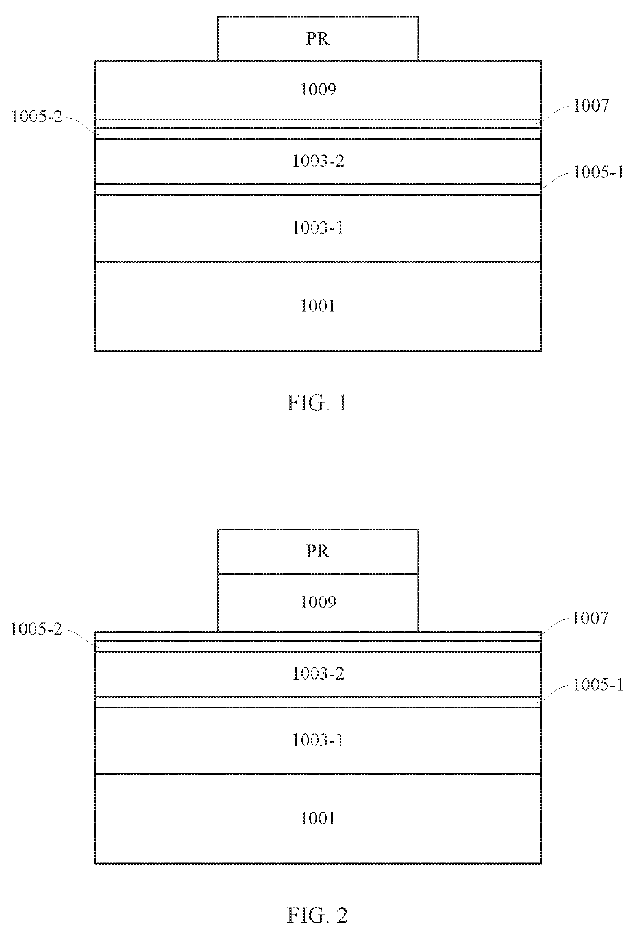
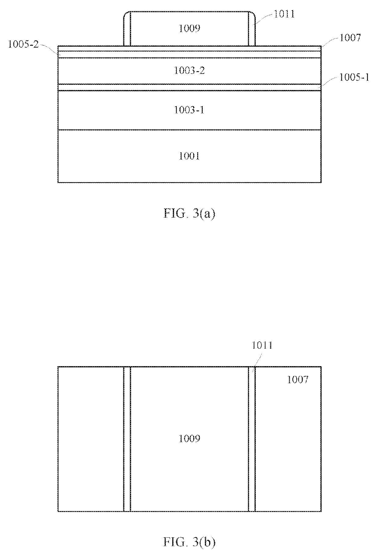
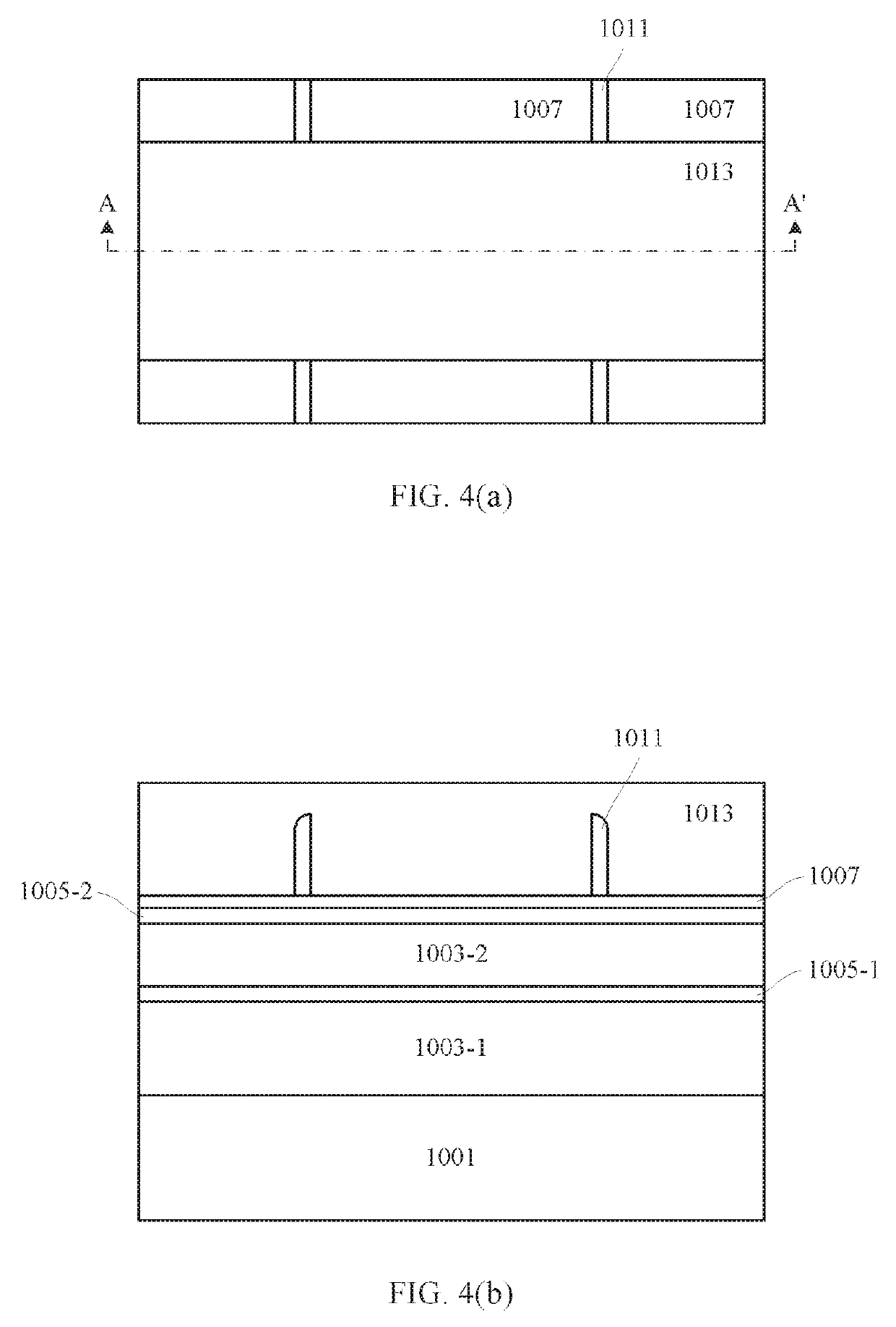
[0015]Hereinafter, embodiments of the present disclosure will be described with reference to the attached drawings. However, it should be understood that those descriptions are provided for illustrative purpose only, rather than limiting the scope of the present disclosure. Further, in the following, descriptions of known structures and techniques might be omitted so as not to obscure the concept of the present disclosure.

[0016]In the drawings, various structures according to the embodiments are schematically shown. However, they are not drawn to scale, and some features may be enlarged while some features may be omitted for sake of clarity. Moreover, shapes and relative sizes and positions of regions and layers shown in the drawings are also illustrative, and deviations may occur due to manufacture tolerances or technique limitations in practice. Those skilled in the art can also devise regions / layers of different shapes, sizes, and relative positions as desired.

[0017]In the contex...


PUM


Abstract

There are provided a nanometer semiconductor device with a high-quality epitaxial layer and a method of manufacturing the same. According to an embodiment, the semiconductor device may include: a substrate; at least one nanowire spaced apart from the substrate; at least one semiconductor layer, each formed around a periphery of respective one of the at least one nanowire to at least partially surround the corresponding nanowire, wherein the semiconductor layer(s) formed around the respective nanowire(s) are separated from each other; an isolation layer formed on the substrate, exposing the at least one semiconductor layer; and a gate stack formed on the isolation layer and intersecting the at least one semiconductor layer, wherein the gate stack includes a gate dielectric layer at least partially surrounding a periphery of respective one of the at least one semiconductor layer and a gate conductor layer.

Description

CROSS-REFERENCE TO RELATED APPLICATION[0001]This application claims priority to Chinese Patent Application No, 201510888321.4, filed on Dec. 7, 2015, entitled “NANOMETER SEMICONDUCTOR DEVICES HAVING HIGH-QUALITY EPITAXIAL LAYER AND METHODS OF MANUFACTURING THE SAME,” which is incorporated herein by reference in its entirety.TECHNICAL FIELD[0002]The present disclosure relates to the field of semiconductors, and particularly to nanometer semiconductor devices having a high-quality epitaxial layer and methods of manufacturing the same.BACKGROUND[0003]With the development of semiconductor devices, it is desirable to manufacture high-performance semiconductor devices such as Metal-Oxide-Semiconductor Field-Effect Transistors (MOSFETs) using a semiconductor material of higher mobility than that of Si. However, it is difficult to form a high-quality semiconductor material of high mobility.SUMMARY OF THE DISCLOSURE[0004]In view of the above, the present disclosure aims to provide, among oth...

Claims


Application Information

Patent Timeline
Patent Type & Authority Patents(United States)
IPC IPC(8): H01L29/786H01L29/06H01L29/423H01L29/10B82Y10/00H01L29/775H01L29/66H01L29/49
CPCH01L29/78684H01L29/66742H01L29/66439H01L29/775H01L29/78651H01L29/4966H01L29/78681H01L29/78696B82Y10/00H01L29/1079H01L29/42392H01L29/0673H01L29/66795H01L29/785
Inventor ZHU, HUILONG
Owner INST OF MICROELECTRONICS CHINESE ACAD OF SCI
Why Eureka
Try Eureka