Light-Emitting Element, Lighting Apparatus, Light-Emitting Device, Electronic Appliance, and Display

a technology of light-emitting elements and lighting devices, which is applied in the direction of discharge tubes/lamp details, discharge tubes luminescnet screens, electric discharge lamps, etc., can solve the problems of deterioration of light-emitting elements and limited advantages of emitting devices including the above-described light-emitting elements, and achieves easy adjustment, low luminance decrease, and high quality display portions

Active Publication Date: 2009-11-19
SEMICON ENERGY LAB CO LTD
View PDF18 Cites 32 Cited by
  • Summary
  • Abstract
  • Description
  • Claims
  • Application Information

AI Technical Summary

Benefits of technology

[0010]An object according to one embodiment of the present invention is to provide a light-emitting element with improved light-emission efficiency. In addition, another object according to one embodiment of the present invention is to provide a light-emitting element or lighting apparatus whose degree of deterioration with a driving time is improved.
[0011]It is another object according to one embodiment of the present invention to provide a light-emitting device or electronic appliance which has a highly reliable display portion.
[0012]It is another object according to one embodiment of the present invention to provide a light-emitting element or lighting apparatus whose emission color is easily adjusted.

Problems solved by technology

Deterioration of a light-emitting element is one of the main reasons why such a light-emitting device including the above-described light-emitting element with many advantages is limited to a partial practical use.

Method used


Image

  • Light-Emitting Element, Lighting Apparatus, Light-Emitting Device, Electronic Appliance, and Display
  • Light-Emitting Element, Lighting Apparatus, Light-Emitting Device, Electronic Appliance, and Display
  • Light-Emitting Element, Lighting Apparatus, Light-Emitting Device, Electronic Appliance, and Display

Examples


embodiment 1

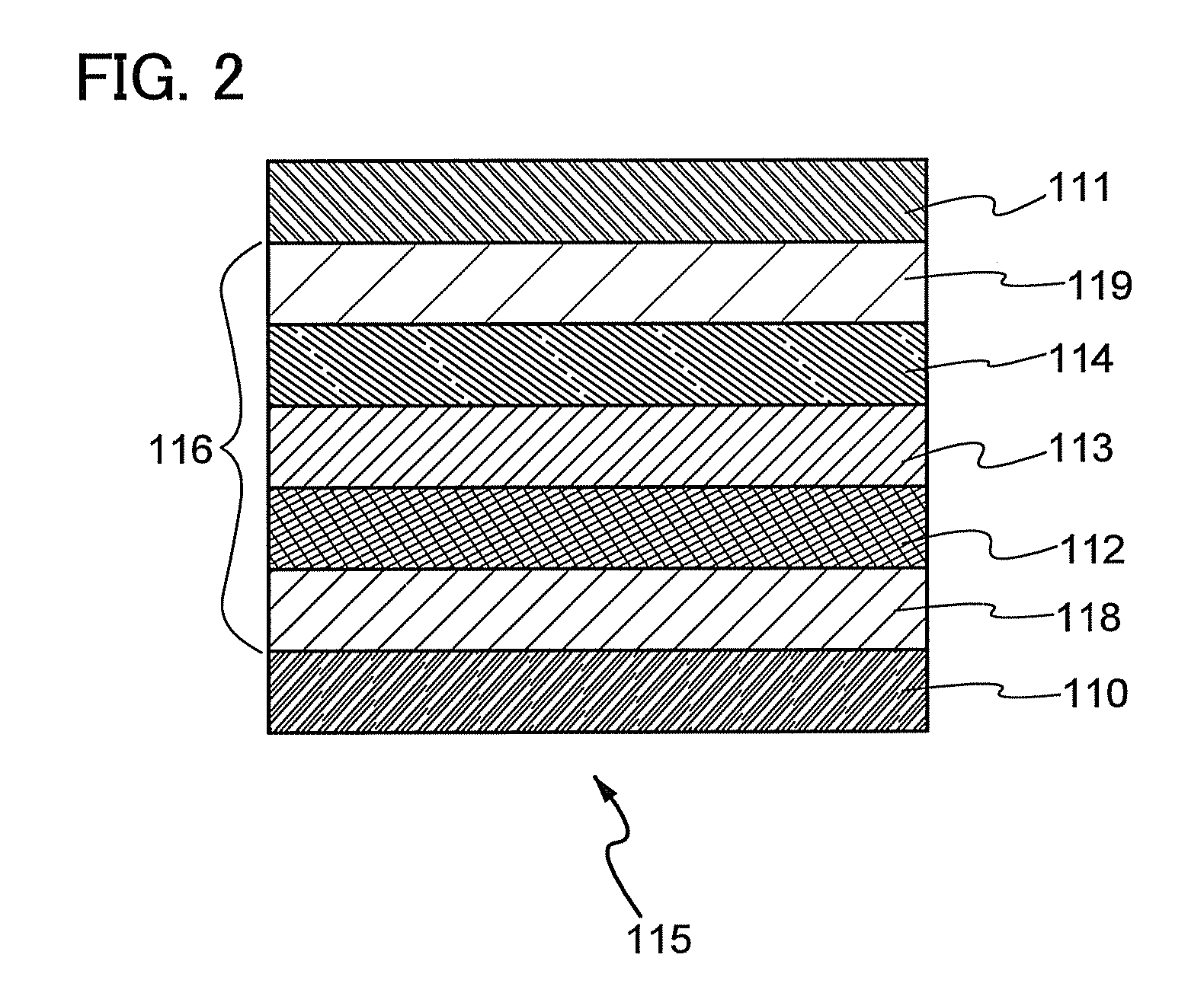
[0058]In disclosing Embodiment 1, first, a conventional light-emitting element 115, which is to be compared with a light-emitting element of this embodiment, is summarized with reference to FIG. 2. In the light-emitting element 115, a layer 116 including an organic compound is provided between an anode 110 and a cathode 111. The layer 116 including an organic compound at least includes a layer serving as a light-emitting layer in which a first layer 112, a second layer 113, and a third layer 114 are stacked in that order over the anode 110. In addition, a functional layer 118 may be provided between the layer serving as a light-emitting layer and the anode 110, and a functional layer 119 may be provided between the layer serving as a light-emitting layer and the cathode 111 as appropriate. The functional layer 118 is, for example, a hole-transporting layer and / or a hole-injecting layer, and the functional layer 119 is, for example, an electron-injecting layer and / or an electron-tran...

embodiment 2

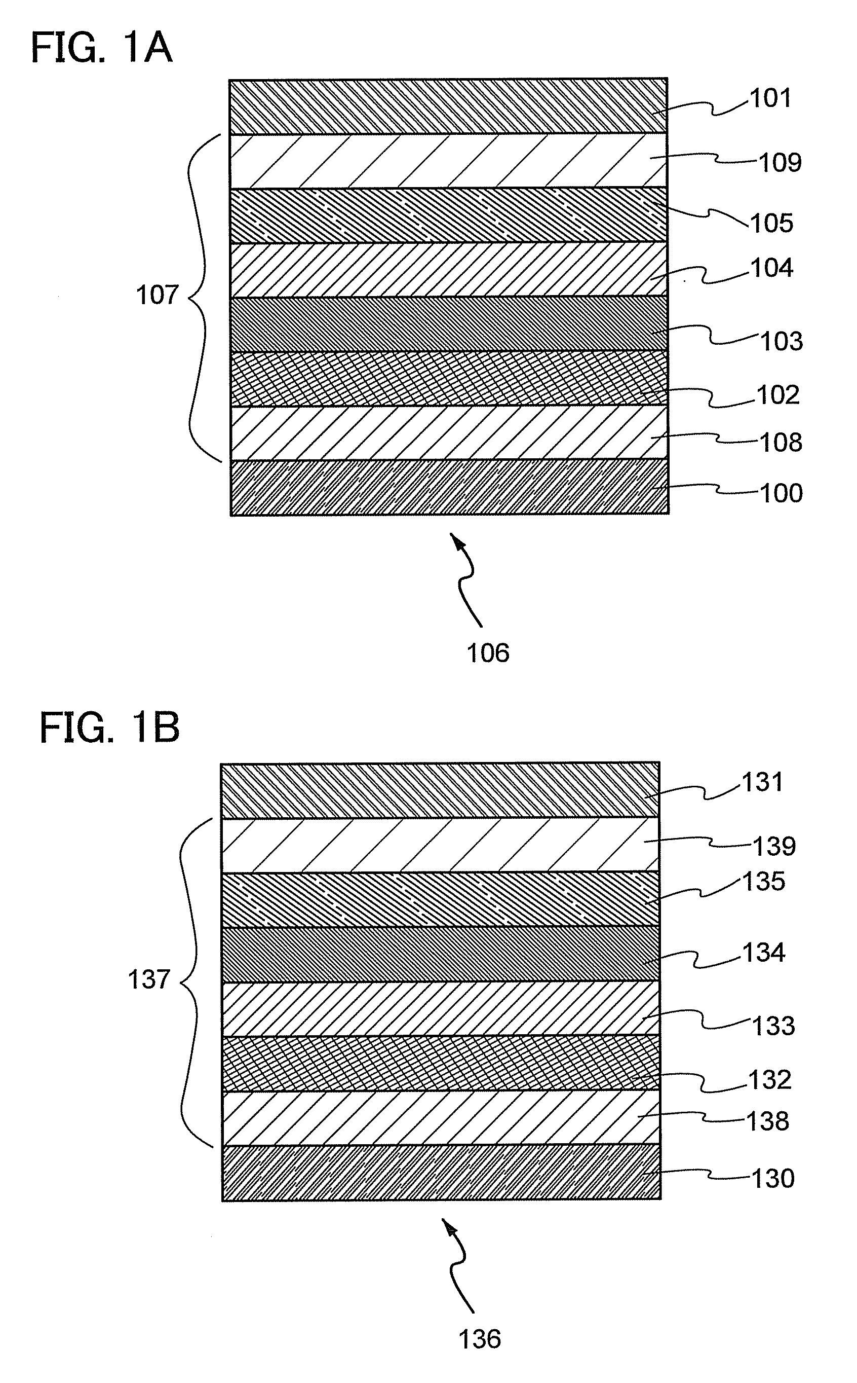
[0073]In this embodiment, a light-emitting element having a structure different from a structure in Embodiment 1 is described with reference to FIG. 1B. A layer 137 including an organic compound is provided between an anode 130 and a cathode 131. The layer 137 including an organic compound at least includes a layer serving as a light-emitting layer in which a first layer 132, a second layer 133, a third layer 134, and a fourth layer 135 are stacked in that order over the anode 130. In addition, a functional layer 138 may be provided between the layer serving as a light-emitting layer and the anode 130, and a functional layer 139 may be provided between the layer serving as a light-emitting layer and the cathode 131 as appropriate. The functional layer 138 is, for example, a hole-transporting layer and / or a hole-injecting layer, and the functional layer 139 is, for example, an electron-injecting layer and / or an electron-transporting layer. Note that the layer 137 including an organic...

embodiment 3

[0084]Next, Embodiment 3 is described. In this embodiment, the light-emitting elements in Embodiment 1 and Embodiment 2 and a method for manufacturing the light-emitting elements are described in specific. Note that an element structure and a manufacturing method described here are just an example, and other known structures, materials, and manufacturing methods can be applied within the scope of the present invention. Although this embodiment is described using the light-emitting element described in Embodiment 1 as an example, this embodiment can also be described using the light-emitting element described in Embodiment 2.

[0085]FIG. 1A schematically shows an example of an element structure of a light-emitting element of this embodiment. The light-emitting element shown in FIG. 1A has a structure in which the layer 107 including an organic compound is provided between the anode 100 and the cathode 101. The layer 107 including an organic compound at least includes a layer serving as...


PUM


Abstract

A layer including an organic compound at least includes a layer serving as a light-emitting layer in which a first layer, a second layer, a third layer, and a fourth layer are stacked in that order over an anode. The first layer includes a first light-emitting substance, the second layer includes a second light-emitting substance, the third layer includes a third light-emitting substance, and the fourth layer includes a fourth light-emitting substance. Emission peak wavelengths of the first light-emitting substance and the fourth light-emitting substance are shorter than an emission peak wavelength of the third light-emitting substance, and the emission peak wavelength of the third light-emitting substance is shorter than an emission peak wavelength of the second light-emitting substance. Each of the first layer, the second layer, and the third layer has a hole-transporting property, and the fourth layer has an electron-transporting property.

Description

BACKGROUND OF THE INVENTION[0001]1. Field of the Invention[0002]The present invention relates to light-emitting elements including an organic compound at least as a part thereof. The present invention also relates to lighting apparatuses, light-emitting devices, electronic appliances, and displays which include the light-emitting element.[0003]2. Description of the Related Art[0004]Development of a light emitting device including a light-emitting element in which a layer including an organic compound is provided between a pair of electrodes and light emission is obtained by current flowing between the pair of electrodes has been advanced. Such a light-emitting device can reduce thickness and weight of a display device in comparison with a display device which is currently called a “thin display device”. Moreover, such a light-emitting device is of a self-emission type, and therefore, has a high level of visibility and high response speed. Accordingly, such a light-emitting device ha...

Claims


Application Information

Patent Timeline
Patent Type & Authority Applications(United States)
IPC IPC(8): H01J1/62
CPCH01L27/3213H01L27/322H01L27/3244H01L51/0052H01L51/5036H01L51/0061H01L51/0065H01L51/0072H01L51/0081H01L51/006H10K59/351H10K59/38H10K59/12H10K85/615H10K85/636H10K85/633H10K85/653H10K85/6572H10K85/324H10K50/125H10K50/11
Inventor USHIKUBO, TAKAHIROSEO, SATOSHIOSHAWA, NOBUHARUYAMAZAKI, SHUNPEI
Owner SEMICON ENERGY LAB CO LTD
Why Eureka
Try Eureka