Photoelectric conversion device and electronic device having the same

Inactive Publication Date: 2009-11-26
SEMICON ENERGY LAB CO LTD
View PDF6 Cites 8 Cited by
  • Summary
  • Abstract
  • Description
  • Claims
  • Application Information

AI Technical Summary

Benefits of technology

[0013]It is an object of an embodiment of the present invention to provide a photoelectric conversion device in which output voltage can be obtained by reducing the adverse effect of the temperature dependence of a diode element even in a condition where temperature changes greatly. It is an object of an embodiment of the present invention to provide a photoelectric conversion device which can be operated with the level of output voltage or the amount of output current used as the level of voltage in the lower limit of detection or the amount of current less than the lower limit of detection even in a condition where weak light which is less than the lower limit of detection of a photoelectric conversion element is detected.
[0025]According to the above embodiment of the present invention, a photoelectric conversion device can be obtained in which fluctuation in the first voltage due to the temperature dependence of a diode element for logarithmic compression can be suppressed. Further, according to the embodiment of the present invention, even in the case where weak light which is less than the lower limit of detection of a photoelectric conversion element is detected, a constant output signal can be obtained.

Problems solved by technology

However, in the case where the logarithmic compression of illuminance is performed using the diode element, there is a problem in that the level of output voltage fluctuates due to the temperature dependence of the diode element and that accurate output voltage cannot be obtained.
Further, in the photoelectric conversion device disclosed in Reference 3, even in the case where weak light which is less than the lower limit of detection is detected using the photoelectric conversion element, the output voltage is amplified; thus, there is a problem in that desired output voltage cannot be obtained.

Method used


Image

  • Photoelectric conversion device and electronic device having the same
  • Photoelectric conversion device and electronic device having the same
  • Photoelectric conversion device and electronic device having the same

Examples


embodiment 1

[0051]In this embodiment, the structure and the operation of a photoelectric conversion device of the present invention are described. Note that in the photoelectric conversion device of the present invention, which is described in this embodiment, a signal related to the amount of incident light, which is obtained from a photoelectric conversion element, is converted into a signal subjected to logarithmic compression and is output outside.

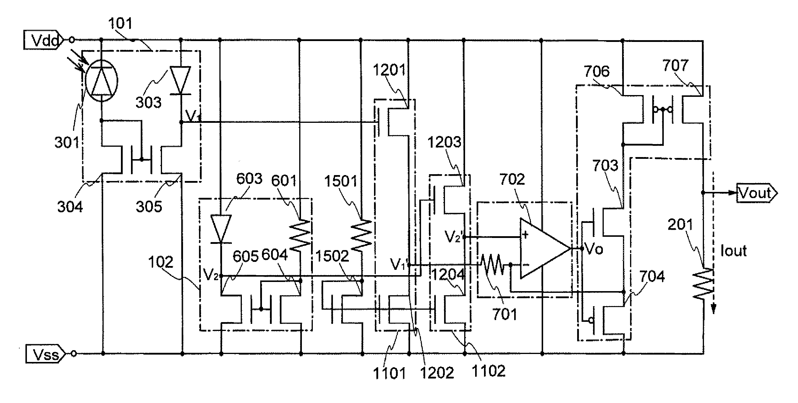
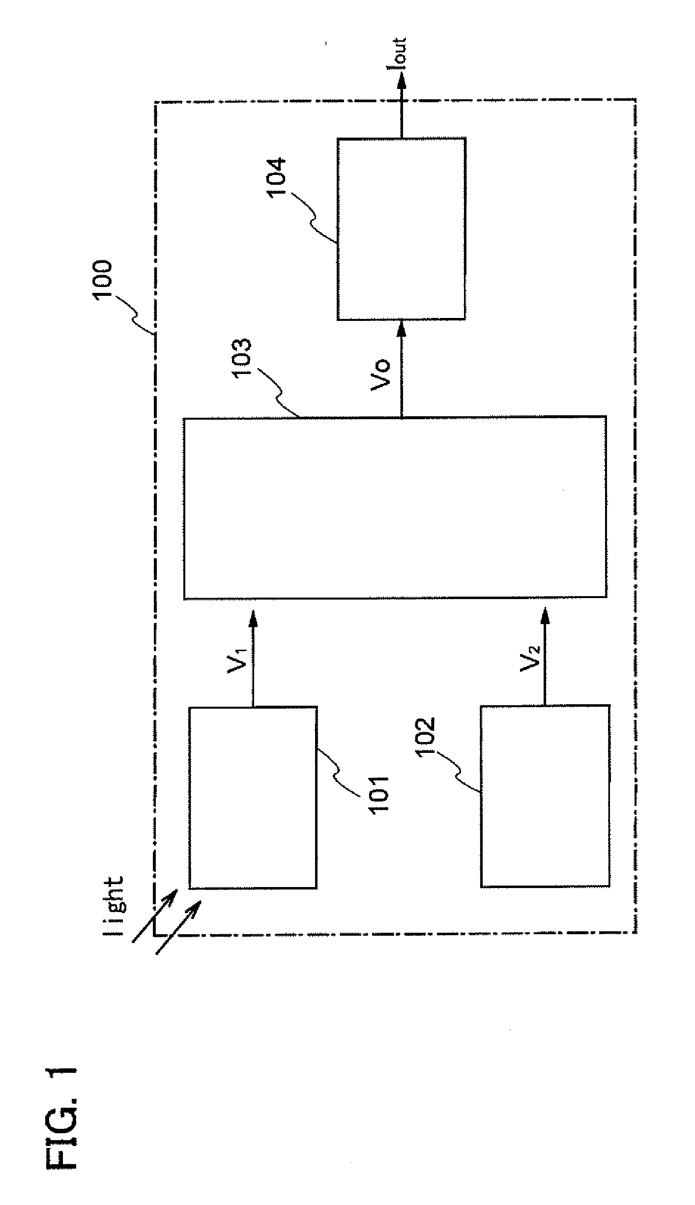
[0052]First, a block diagram of a photoelectric conversion device is described. A photoelectric conversion device 100 illustrated in FIG. 1 includes a photoelectric conversion circuit 101, a reference voltage generation circuit 102, an arithmetic circuit 103, and an output circuit 104. The photoelectric conversion circuit 101 is a circuit for outputting first voltage V1 subjected to logarithmic compression by one of terminals of a first diode element in accordance with photocurrent flowing to a photoelectric conversion element. In addition, the re...

embodiment 2

[0092]In this embodiment, a specific structure in the case where the first voltage V1 and the second voltage V2 are used as signals amplified in a source follower circuit instead of using the first voltage V1 and the second voltage V2 which are input to the arithmetic circuit 103 in the photoelectric conversion device 100 described in the above embodiment is described. Note that in this embodiment, portions described in Embodiment 1 are denoted by the same reference numerals as in Embodiment 1, and description thereof is omitted.

[0093]A photoelectric conversion device 1100 illustrated in FIG. 11 includes the photoelectric conversion circuit 101, the reference voltage generation circuit 102, the arithmetic circuit 103, the output circuit 104, a first amplifier circuit 1101, and a second amplifier circuit 1102. The photoelectric conversion device 1100 illustrated in FIG. 11 differs from the photoelectric conversion device 100 described in Embodiment 1 in that the first amplifier circu...

embodiment 3

[0100]In this embodiment, a layout example of each circuit is described with reference to a block diagram of a photoelectric conversion device. FIG. 14 is a block diagram of the photoelectric conversion device, which illustrates the layout of each circuit in the circuit illustrated in FIG. 12 in Embodiment 2. In the photoelectric conversion device 1100 illustrated in FIG. 14, the photoelectric conversion element 301, the resistor 601, the first diode element 303, the second diode element 603, the first amplifier circuit 1101, the second amplifier circuit 1102, the resistor 701, the operational amplifier 702, and the output circuit 104 are illustrated. Note that in FIG. 14, a terminal to which the high power supply potential Vdd is applied, a terminal to which the low power supply potential Vss is applied, and a terminal for outputting the voltage Vout obtained in the photoelectric conversion device to the outside are also illustrated.

[0101]As described in the above embodiment, in th...


PUM


Abstract

The photoelectric conversion device includes a photoelectric conversion circuit for outputting photocurrent generated in a photoelectric conversion element as output voltage subjected to logarithmic compression by a first diode element, a reference voltage generation circuit for outputting reference voltage subjected to logarithmic compression by a second diode element in accordance with the amount of current flowing to a resistors an arithmetic circuit for outputting an output signal obtained by amplifying a difference between the output voltage output from the photoelectric conversion circuit and the reference voltage output from the reference voltage generation circuit, and an output circuit for outputting current corresponding to the logarithmically-compressed output voltage output from the photoelectric conversion circuit by the output signal.

Description

BACKGROUND OF THE INVENTION[0001]1. Field of the Invention[0002]The present invention relates to photoelectric conversion devices and electronic devices having the photoelectric conversion devices. In particular, the present invention relates to photoelectric conversion devices in which output signals are logarithmically converted and electronic devices having the photoelectric conversion devices.[0003]2. Description of the Related Art[0004]A large number of photoelectric conversion devices generally used for detecting electromagnetic waves are known. For example, photoelectric conversion devices having sensitivity to ultraviolet rays to infrared rays are generally referred to as optical sensors. Among optical sensors, an optical sensor having sensitivity to a visible light region with a wavelength greater than or equal to 400 nm and less than or equal to 700 nm is particularly referred to as a visible light sensor. A large number of visible light sensors are used for devices which ...

Claims


Application Information

Patent Timeline
IPC IPC(8): H03F3/08
CPCH03F3/08
Inventor KOYAMA, JUNHIROSE, ATSUSHI
Owner SEMICON ENERGY LAB CO LTD
Why Eureka
Try Eureka